Get in Touch with Saiweiglass



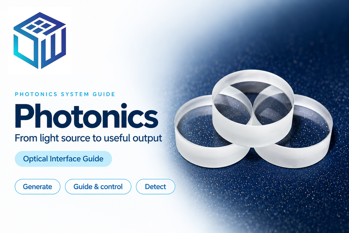
Photonics is the science and technology of controlling, generating, and detecting light. It connects a light source to a useful output: data transmitted through a fibre, an image captured by a camera, or a measurement taken by a sensor.
A clear component label rarely explains the whole job. A window can protect a receiver while changing the light reaching it; a photonic chip can move information between electronic processors. Following the light through the system helps understand the differences and turns a wide technology question into design and purchase decisions.
By Dd · Updated November 2026
Quick Specs: photonics functions
- Working medium: light, including visible and invisible wavelengths.
- Core functions: generate, guide, modify and detect an optical signal.
- Typical outputs: transmitted information, an image, a measurement or delivered energy.
- Component selection: match the spectrum, optical geometry and receiving device to the application.
Photonics: light as a signal, a probe and a tool
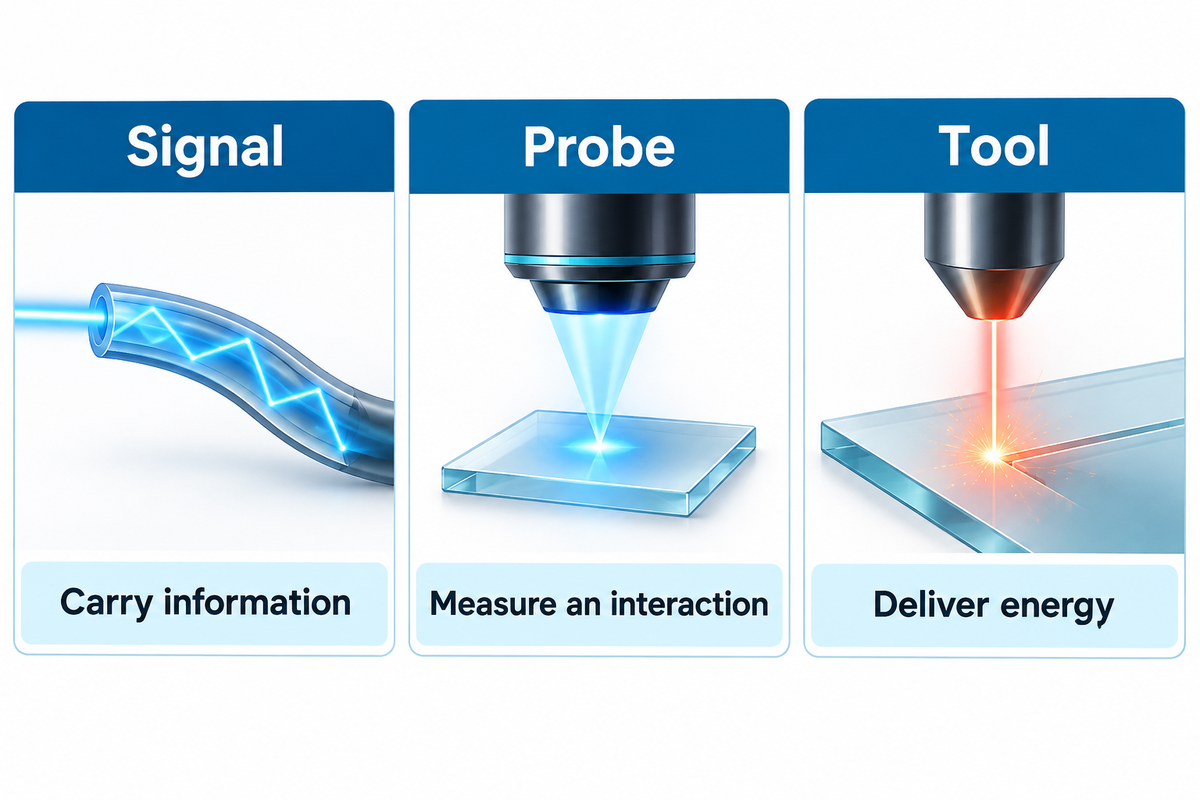
Photonics uses light to transport information, study, or affect an object, and deliver energy. The same medium is used for different functions: communication preserves encoded data, sensing measures a change, and laser processing delivers energy to a material. It’s the function that determines the properties of light that need to be retained for the journey.
According to the University of Central Florida, photonics is the study of light and its use in light-based technologies. NASA’s 2024 report describes laser signals transmitted from Earth to its Psyche mission over about 460 million kilometers. The field includes infrared and ultraviolet light as well as visible light. Electromagnetic radiation that the eye can’t see can still carry information to a suitable detector.
- Signal: a transmitter changes the light to encode information; a receiver recovers it.
- Probe: light interacts with a sample, and the instrument measures what comes back or passes through.
- Tool: absorbed light transfers energy, as in laser material processing.
Consider a camera inspecting an object along a production line. There are a number of factors affecting the image. Illumination, lens and sensor all play a role, but solve different problems. Brighter illumination may reveal detail, while an unwanted reflection can obscure it. Describing the type of image to be captured determines the type of illumination to be used.
Photonics vs optics and electronics
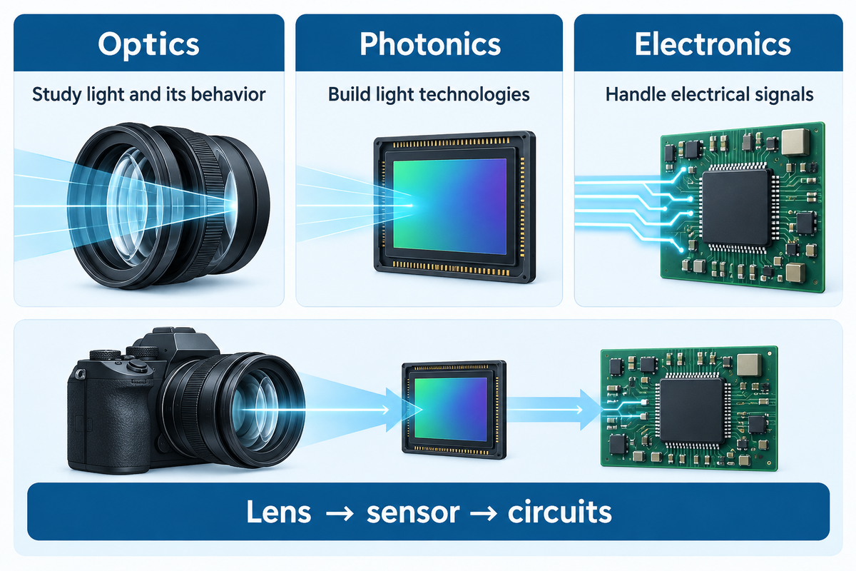
Photonics and optics both study light and work with devices; electronics handles electrical signals. Optoelectronics studies the conversion of light to electrical energy, or electrical energy to light. A camera is an excellent example; its lens forms an image, its sensor captures the image using light, and its circuits read and process the image.
What is the difference between photonics and optics?
Optics studies light and its behaviors, and photonics focuses on light technologies. The distinction is one of emphasis, not a strict boundary. Many photonic systems can be explained using rays or waves without a quantum description.
The University of Rochester’s explanation of optics identifies geometrical, physical and quantum descriptions. Rays are used to describe focusing and refraction. Waves are used to explain diffraction and interference. The photon description becomes essential for the phenomena involving discrete light-matter interactions.
“Branch of physics that deals with the optical-to-electric and electric-to-optical transducers.”
From a buyer’s perspective, these names describe responsibilities in an assembly. An optic, for example, a lens, redirects light. A photodetector converts light to an electric signal. The board interprets that signal. Specifying the lens leaves the detector and electric components undefined.
Optical components in a working photonic system
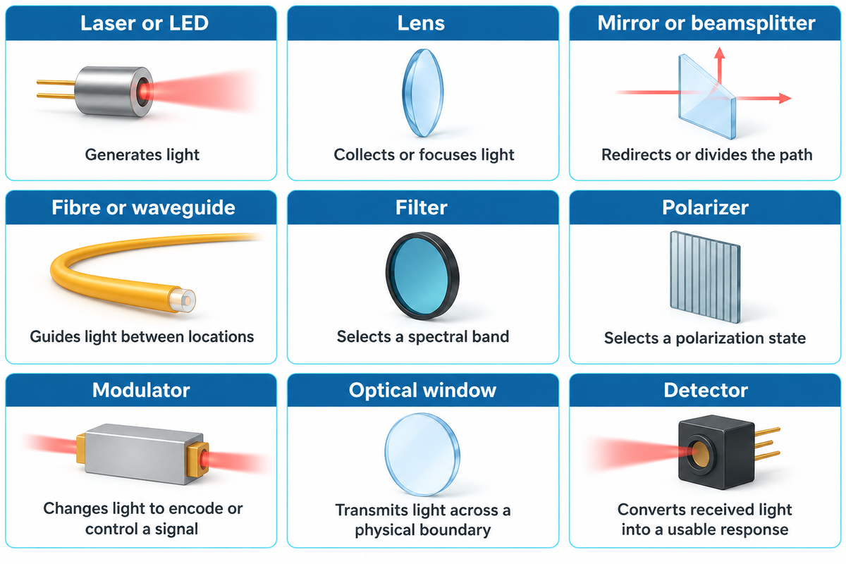
Along a path of light, optical components perform different functions: emission, routing, selection, modulation and detection. Choosing compatible components means examining what leaves one component against what the other accepts. The type of light, beam geometry, and the level of the signal at the interface are of great importance for all components along the path.
| Component type | Function | Interface to specify |
|---|---|---|
| Laser or LED | Generates light | Emission spectrum and output geometry |
| Lens | Collects or focuses light | Beam size, focus and field of view |
| Mirror or beamsplitter | Redirects or divides the path | Angle, polarization and coating band |
| Fibre or waveguide | Guides light between locations | Coupling geometry and supported optical mode |
| Filter | Selects a spectral band | Passband, blocking and incidence angle |
| Polarizer | Selects a polarization state | Orientation and transmitted state |
| Modulator | Changes light to encode or control a signal | Drive signal and required modulation |
| Optical window | Transmits light across a physical boundary | Clear aperture and assembled optical performance |
| Detector | Converts received light into a usable response | Spectral response, signal range and readout |
A single component can perform more than one of these optical functions.
Filters illustrate why the interface matters. A filter may pass the desired band at one incidence angle and shift its spectral response when tilted. In fluorescence microscopy, excitation light and the weaker emitted light follow carefully separated paths. The Florida State University interference-filter primer explains how thin-film layers control that selection.
A fibre optic connection adds a different handoff: coupling light into a guided mode. Free-space and fibre alignment therefore require different drawings and test setups. On a photonic circuit, a resonator can select a narrow band while a grating can couple light between paths; these structures belong to the design of the circuit rather than the enclosure drawing.
Optical control also changes what a component must deliver. A modulator can alter the amplitude or phase of a passing wave. The route can also be changed with a switch. Wavelength tunability concerns where a source operates in the spectrum. For a tunable source, the downstream filter and detector must suit the desired settings.
Detector selection also separates brightness from usefulness. For the detector to be useful, it must respond to the wavelength of light it receives; that is, have the correct spectral sensitivity. Quantum efficiency describes the process of conversion in a detector, and the effects of noise and readout determine the final measurement. A low-light imaging system must have an adequate optical signal and an appropriate electronic readout.
Photonics applications from communications to marine sensing
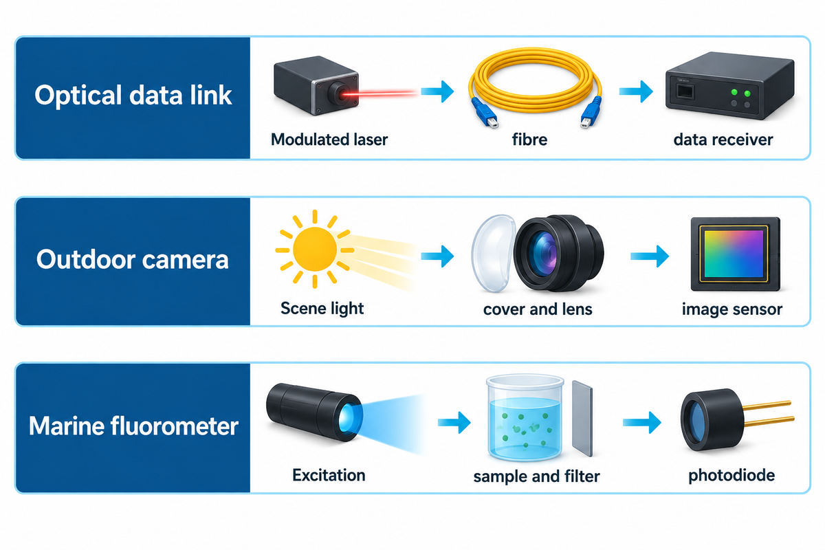
Photonics applications vary in the result they extract from light. Communication links recover encoded data; cameras create spatial images; and fluorescence sensors measure light emitted after excitation. Tracking each application from source to output identifies the components it requires, and shows if an exposed optical window is part of the measurement path.
What are examples of photonics?
Examples include optical-fibre communication, camera imaging, laser manufacturing and fluorescence sensing. Displays emit or redirect light toward a viewer, while a solar cell converts absorbed light into electrical energy. The University of Michigan’s optics and photonics research overview connects communications, imaging and sensing with the underlying optical technologies.
Lidar adds a ranging task: the receiver uses reflected light to measure distance. A high-resolution camera needs spatial detail in the captured image. As such, the quality of the imaging path determines acceptance. These different outputs explain why the same clear cover can require different optical tests in two instruments.
Signal-Path Handoff Map
| Application | Source | Path and control | Receiver/output | Window’s role |
|---|---|---|---|---|
| Optical data link | Modulated laser light | Waveguide and optical fibre | Receiver recovers data | No separate environmental window is inherent to a guided link |
| Outdoor camera | Scene illumination | Cover, lens and imaging path | Image sensor produces image data | Cover transmits the scene across the housing boundary |
| Marine fluorometer | Excitation light | Sample interaction and emission filtering | Photodiode detects emitted light | Exposed optical interfaces must preserve the measurement path |
The communication and marine paths use the Intel Corporation Silicon-photonics document and the WET Labs ECO FLNTU manual. The camera path presents one possible system configuration. For range comparisons of lidar, TI recommends measuring in the same environmental conditions because environmental factors affect range.
Imagine an outdoor camera being converted for a marine instrument enclosure. The first prototype creates a clear image on the workbench, and the purchasing team requests the same glass shape in production. The optical engineer sees a different task: the installed cover must transmit light across the camera’s viewing cone, the bezel must be outside that cone, and reflections from the actual lighting must be checked. The enclosure engineer owns the sealing and mechanical loads. Quality Assurance needs a repeatable image test with the cover mounted. Keeping these responsibilities on one drawing package means a visually acceptable loose part won’t become the only acceptance criterion for the assembled instrument.
A marine fluorometer is a good example. The WET Labs ECO FLNTU manual mentions blue excitation, a red emission filter, and a silicon photodiode. The useful signal is the sample’s response, so background light and excitation leakage affect the signal, as well as transmission. Its optical task is different from making a display readable in the presence of ambient light.
For the display task, transflective display design makes use of both transmitted and reflected light. Our outdoor and marine display glass application discusses this in more detail.
Optical windows translate the application into specifications
Optical windows should be specified based on the light they need to transmit and the assembly they join. The pertinent considerations include wavelength, incidence angle, clear aperture, surface condition and mounting. If both media are air, an optical glass window has air-glass interfaces; if one is air and one is water, the optical interfaces change.
Edmund Optics’ literature describes the difference between transmitted wavefront error and surface flatness. Performance depends on the quality of the material and the stress condition of the mount, in addition to the requirements defined by the application. Material selection belongs alongside those requirements; the separate BK7 optical glass guide covers that specific material.
A filled window handoff example
Consider a visible-light camera designed for outdoor inspection with an air-filled enclosure. This example connects engineering, procurement and quality assurance requirements; project acceptance limits come from the camera design.
| Requirement | Camera example | Evidence to deliver |
|---|---|---|
| Spectrum | Visible illumination and detector response | Transmission curve across the operating band |
| Incidence angles | Centre and edge rays from the camera’s viewing cone | Coating performance over those angles |
| Clear aperture | Unobstructed light path inside the bezel | Drawing showing optical area, edge and masked rim |
| Polarization | No intentional polarizer in the baseline assembly | Document the polarization condition used in testing |
| Media at each face | Air outside and inside for the baseline test | Separate wet-face evaluation if immersion is intended |
| Surface and wavefront | Image-forming path through the mounted cover | Specified surface inspection and assembled image check |
| Background | Reflections from enclosure lighting | Image comparison with source positions recorded |
| Mounting | Cover retained in the production bezel | Optical check in the final mounting condition |
| Exposure and cleaning | Outdoor contamination and the intended cleaning process | Repeat optical checks after agreed exposure and cleaning |
The example illustrates optical window selection, as well as the management of interface reflections and contamination. Edmund Optics states that window surface quality and surface flatness affect optical performance.
For fluorescence measurements, add a blank-background test using the intended excitation and collection bands. Fluorescence from a substrate or coating can falsely contribute to the measured signal and affect the performance of the system. This is especially true for a weak sample signal. A background test is distinctly different from a normal transmission test.
ISO 10110-7:2017, the third edition confirmed in 2022, specifies how acceptable surface imperfections are indicated within a test region of finished optical elements and assemblies.
Keep optical acceptance separated from enclosure qualification. The mechanical and thermal properties of glass influence the mechanical design, and sealing and pressure performance belong to the complete enclosure and the tests specified therein. Manufacturing imperfections should be assessed against the defined optical test region and drawing requirements.
Optical signal to noise ratio and hidden interface losses
Improving the signal to noise ratio (S/N) makes the desired optical signal easier to detect. Signal attenuation along the transmission path and interference from unwanted reflections are different effects to diagnose before increasing the brightness of the signal source. Diagnosing the mechanism matters: increasing source brightness will not necessarily remove an unwanted optical path or background emission.
A single-interface reflection calculation
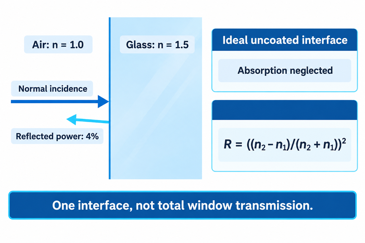
Take an ideal uncoated interface between air with refractive index 1.0 and transparent glass with index 1.5. In the case of normal incident light, absorption is neglected. The University of Texas Fresnel relations give the reflected power fraction as R = ((n₂ − n₁)/(n₂ + n₁))². Substituting the inputs gives ((1.5 − 1.0)/(1.5 + 1.0))² = 0.04, or 4%. For an engineer comparing covers, the value identifies a reflection before discussing any material absorption. It’s a single-interface calculation and not the measured total transmission of a complete window. A coated surface or an oblique ray requires the respective interface model and operating conditions.
Texas Instruments’ optical distance-sensing application note mentions ambient light shot noise and multipath interference. Enlarging the field of view or receiver aperture can allow more signal and more unwanted light to enter. A reflection that takes a longer route can also alter the final result.
- Signal falls after handling: inspect the optical surface and compare against the clean baseline.
- Readings change with illumination: examine ambient-light admission, filtering and receiver geometry.
- Distance shifts after fitting a cover: investigate cover reflections, mechanical geometry and the sensor’s calibration procedure.
- A fluorescence blank becomes brighter: test substrate and coating background under the actual excitation.
NASA’s optical contamination practice explains how throughput loss and scattering are caused by deposits and particles. A study by the Society of Vacuum Coaters indicates optical-element fluorescence as one of the factors limiting low-background measurements. The first passage discusses cleanliness control; the other discusses a measurement of an appropriate blank.
An Arduino forum discussion from February 2021 cites an example of a user covering a time-of-flight sensor and reporting that calibration code apparently didn’t affect the readings. Checking that calibration values were properly applied is a different task from checking the glass. For component-level inspection, see our glass inspection methods.
Optical coating cost: compare the same specification
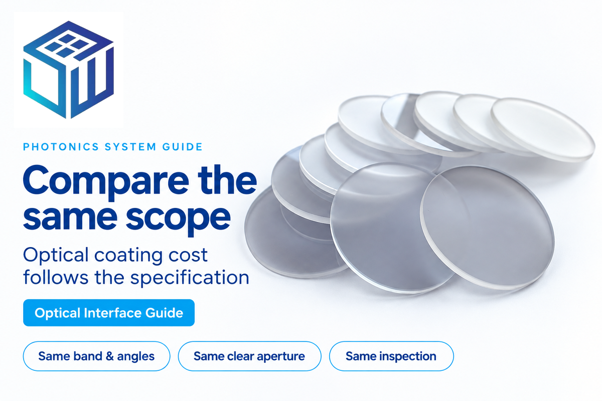
Optical coating cost reflects the performance and verification being purchased, not just the glass dimensions. Comparing quotations starts with matching the wavelength band, angular range and clear aperture. Further comparison depends on surface requirements, quantity, and inspection records. For the lowest unit price to be meaningful, the requirements have to match.
An example in the anti-reflection coating guide by RP Photonics uses a numerically optimized coating for 1064 nm and 532 nm on BK7. These are design wavelengths. A quote for a broad visible band or a different angular range describes a different optical job, even if the substrate dimensions are identical.
Consider an example where a buyer reviews two quotations for a camera cover. One quotation includes a coating curve measured at normal incidence and a visual surface check. The other includes performance over the camera ray-angle range and inspection of the mounted clear aperture. Procurement sees different prices, while engineering sees different deliverables. Before awarding the order, the team asks both suppliers to quote the same band, angles, aperture and acceptance documentation requirements. Finance can then compare the cost of accepted parts without treating missing inspection work as a saving. If there are angular requirements that don’t serve any ray in the real design, engineering can remove them and compare the scopes.
- Freeze the optical requirement — record the operating band, ray angles and required clear aperture.
- Align the inspection package — specify the same measurement conditions, sampling and delivered records.
- Compare accepted-part scope — include agreed coating, inspection and rework responsibilities in both offers.
Edmund Optics also cautions that over-tolerancing a window can add unnecessary cost. Remove requirements that don’t serve the optical design before requesting production price. Our anti-reflective coating services are relevant when the required deliverable is a fabricated and coated glass.
Photonics companies: match the supplier to the component
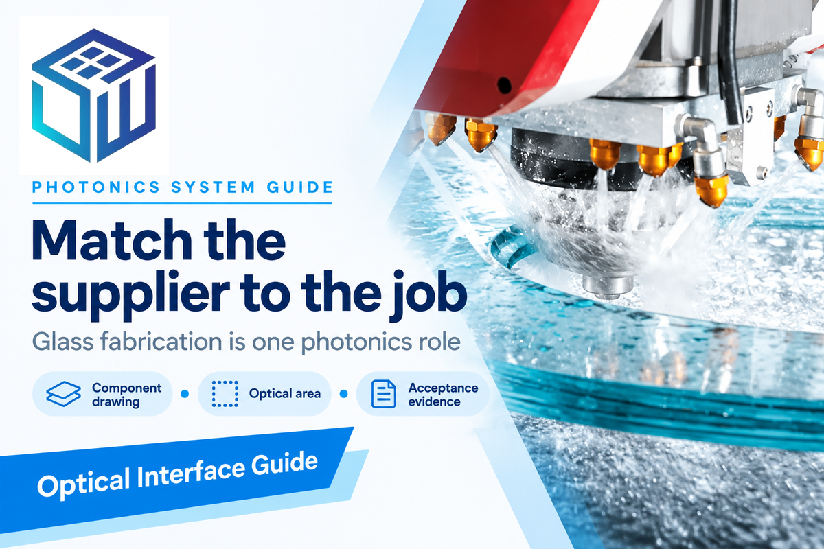
Photonics companies supply different elements of the system, including light sources, optical circuits, detectors, optics and sub-systems. Some cover different roles. The useful distinction is the deliverable and its acceptance test: different manufacturing capabilities and interfaces are required for a wafer process, a packaged transmitter and a finished glass window.
The MIT Integrated Photonics Systems Roadmap provides a clear link of materials and components to system integrators and end-users. The supply-chain view helps a buyer route a request to the right team to consider the actual component.
- Laser supplier: IPG Photonics supplies fibre lasers. The handoff concerns the source and delivery characteristics needed by the application.
- Detector supplier: Hamamatsu lists silicon and InGaAs photodiodes, arrays and amplifier modules. The handoff concerns spectral response, signal level and the receiver circuit.
- Photonic foundry: LIGENTEC describes silicon-nitride process platforms for integrated photonics. The handoff concerns the circuit design and fabrication platform.
- Optical interconnect provider: Intel describes photonic and electronic integrated circuits used for data connections. Packaging and the electronic interface are part of the system.
- Glass fabricator: SW Glass lists cutting, CNC processing, printing, strengthening and AG/AR/AF surface processing. The handoff concerns the glass drawing, optical area, coating and inspection scope.
For a window request, please provide the component drawing along with the system-to-window requirements. The drawing defines the part; the application requirements identify which surfaces and areas perform optical functions. Together, they help fabricators assess custom optical glass components with fewer assumptions about the source or detector.
Comparing companies and countries by the job they do
For a buyer asking who leads photonics, compare companies in the relevant segment: laser sources, detectors, integrated circuits or fabricated optics. The ones listed above are the actual suppliers. A component’s wavelength range, interface and test evidence are more appropriate criteria for shortlisting than a ranking that integrates the four elements.
For the country question, China had the largest global photonics market share in the 2019–2022 research summarized by Photonics21: 32%, compared with Europe’s 15%. Those are historical market figures. The same summary identifies European strengths in industrial photonics, instrumentation and healthcare, so market size and leadership in a particular technology answer different questions.
Silicon photonics and the limits of replacing electronics
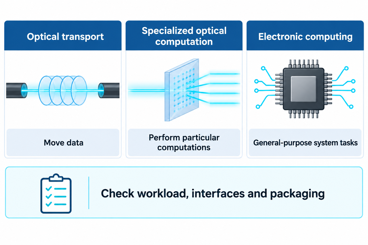
Silicon photonics integrates optical functions on a semiconductor platform, often alongside electronic circuits. Its established role in data networking is moving data; specialized optical processors can perform particular computations. Evaluating a product therefore starts with the workload and interfaces: data transport, optical processing and general-purpose electronic computing are different system tasks.
Is Nvidia investing in photonics?
Yes. The official website of NVIDIA mentions photonics for data center networking. The photonics offerings Quantum-X and Spectrum-X use co-packaged optics around electronic switch ASICs.
Optical transport and specialized computation
Optical computation is also real research. A 2024 Nature Photonics experiment showcased a specialized integrated coherent optical neural network with six neurons and three layers, performing all-optical linear and nonlinear functions with a reported latency of 410 ps.
Nonlinear optical behavior occurs when a material’s response is not proportional to the applied optical electric field. This nonlinearity allows functions beyond simple transfer: frequency mixing and harmonic generation can create new optical frequencies. Source constraints and loss remain challenges in engineering.
Ultrafast optical science helps explain processes on very short time scales. Michigan identifies it and terahertz generation as focused research areas. The former relates to time. The latter concerns a region of the electromagnetic spectrum.
Industry outlook: integration makes interfaces more important
As MIT’s May 2026 roadmap meeting highlighted, the tight integration of electrical-photonic systems brings practical constraints (e.g. packaging) that require a systems integration perspective. For a project entering development, the buying decision should address how the optical connection, electrical drive and thermal management components will be assembled and tested.
Miniaturization presents a further set of trade-offs. Nanophotonics studies optical behavior at the nanoscale, where a patterned nanostructure can confine or redirect a field. The Yale review of optical materials for nanophotonic response illustrates why material performance must be assessed based on the desired function and frequency.
For example, the Yale review relates a nanoparticle’s resonance to its shape and material. This makes geometry a factor in selecting the resonant element, rather than treating the material name alone as a complete specification.
For instance, a plasmon couples light to a collective electron motion and can support subwavelength confinement. Absorption then competes with the desired optical response, while dielectric structures also face radiative losses. Graphene and similar materials therefore need to be assessed based on application requirements; a high response in a particular spectral region doesn’t guarantee a low-loss result in another region.
The Yale review considers material behavior over different regions of the spectrum, including the mid-infrared, and discusses near-field response (fields in the vicinity of a structure). For designs that require strong local interaction, assess materials based on near-field response; a material chosen for distant transmission may need a different performance criterion. For a device intended to modify the spontaneous emission rate, the relevant measure is that rate rather than window transmission.
The research directory mentions engineered metamaterials and metasurfaces. Their structure is part of the optical design, so assessing a metamaterial requires the intended geometry as well as the material name. The directory separates low-dimensional semiconductor research and photoacoustic sensing, and so illustrates how wide the field is beyond conventional lenses and windows.
A scalable photonic circuit must fit a repeatable fabrication and packaging process. A buyer comparing integrated photonic circuits should ask which functions are on-chip and which still require external components. Keep the window and coating requirements for the optical path that passes through the package or housing.
Photonics FAQ
What is photonics engineering?
Photonics engineering converts optics into functioning systems and devices.
The work can include optical design, source and detector selection, integrated-circuit development, packaging, testing and calibration. A useful engineering specification relates the desired output to the whole system that generates it. For an imaging device, for example, consider the illumination, the lenses, detector, electronics and packaging, and also consider acceptance tests that represent the system as an integrated device.
How close are we to photonic chips?
Photonic chips are already deployed in optical communications: Intel reports shipping more than 12 million photonic integrated circuits (PICs) for data center networking. Intel reports that these PICs, embedded in pluggable optical transceivers, contain over 45 million on-chip lasers. Other optical computing circuits have also been demonstrated; maturity is function-specific.
Intel’s silicon-photonics products illustrate communication, while the Nature Photonics neural network experiment illustrates a computation. Neither category supplies every function of a conventional computer. A product assessment should identify the actual workload, the remaining electronic circuitry, packaging, and performance measured for the complete intended function.
What is Intel doing in photonics?
Intel develops silicon-photonics technology for optical data links, including photonic integrated circuits and optical compute interconnect.
Its public overview describes optical components working with electronic integrated circuits for drive and control functions. The optical path carries data between various elements of a computing system, and electronic components continue to supply processing and other functions. The important questions for a buyer concern the connection architecture, electrical interfaces, optical packaging, and the requirements of the target system.
Are photonics lasers?
Lasers are one part of photonics.
The field includes light guiding components, filters, imaging systems and detectors. In many situations, light from the surrounding scene is used. The source of light follows the function; a camera doesn’t become a laser system, just because it employs photonic components.
Is photonics related to quantum computing?
Photonics can support quantum computing and quantum information research, where light carries or interacts with quantum states.
Most everyday communication, imaging and lighting applications do not involve quantum computing. Quantum optics examines the behavior of light and matter at the quantum level, while photonics also includes technologies sufficiently described by classical waves and rays. Photonics also includes industrial components such as windows, filters and camera lenses.
Do photonics use copper?
Photonic equipment can contain copper electrical connections.
Optical fibres are light-carrying elements, while electrical conductors can supply power and provide interconnections to control or readout circuits. Replacing a specific data link with an optical connection doesn’t remove all the electrical connections in surrounding equipment.
Who buys photonics products?
Purchasers of photonics products include communication equipment manufacturers, instrument builders, automation system builders, imaging system and apparatus builders, and research laboratories.
The order may be for a laser, detector, photonic circuit, or a fabricated window. Starting from the function and interface specification enables the supplier to assess the right deliverable. A custom glass inquiry requires the optical path and assembly conditions, and a circuit inquiry requires the fabrication platform and packaging requirements.
Key takeaway
Trace the source, path and output first, then specify each interface and assign its acceptance test.
Discuss the glass in your optical path
For a fabricated glass window or cover in your project, provide drawing(s), operating spectrum, viewing geometry, and inspection requirements to SW Glass. The example in the window handoff section provides a baseline to discuss the same item with the optical engineer, buyer, and quality personnel.
Our perspective on the optical interface
SW Glass approaches this topic through glass fabrication and surface processing. This document links that component work to the photonics system so that a window request includes the light path, assembly and inspection conditions. Its examples provide the rationale for certain design decisions. They aren’t descriptions of completed customer work. Technical and product descriptions are given attribution.
References & Sources
- What Is Optics & Photonics? University of Central Florida, CREOL.
- What Is Optics? University of Rochester.
- Optoelectronics IUPAC Gold Book.
- Optics & Photonics University of Michigan.
- Interference-filter principles Florida State University, Molecular Expressions.
- ISO 10110-7:2017 International Organization for Standardization, public catalogue scope.
- Fresnel Relations University of Texas at Austin.
- Contamination Control of Space Optical Systems NASA.
- Using Optical Interference Filters to Measure Autofluorescence in Substrates and Coatings Society of Vacuum Coaters, 2021 abstract.
- Integrated Photonics Systems Roadmap International MIT Microphotonics Center, 2026 public overview.
- Integrated optical neural-network experiment Nature Photonics, 2024 public abstract.
- Optical materials for maximal nanophotonic response Hyungki Shim, Zeyu Kuang and Owen D. Miller, 2020.