Get in Touch with Saiweiglass


ITO Coating Process & Cost Breakdown: Magnetron Sputtering, Sheet Resistance Tuning

What’s the cost of ITO coating? ITO coating process and cost is a procurement specification for how indium tin oxide is deposited on glass, how the transparent conductive film is tuned, and how much inspection risk the buyer asks the supplier to absorb. For buyers, the RFQ should define a sheet-resistance window such as 10 ohms/sq or 100 ohms/sq, a 5 mm x 5 mm contact-clearance rule where needed, the optical target, and the inspection map. The quote should be derived from specifications, not guessed from generic indium spot prices.
Answer: ITO coating cost is driven by format, coating area, target sheet-resistance, transmittance, uniformity, target exposure, patterning or masking, bus bars, finishing quality, yield, volume, and delivery time. Finished pricing requires drawings and an RFQ because the same nominal ohms/sq can mean very different process windows.
Cost boundary: this article describes quote logic and cost drivers. It does not publish a universal ITO coating price list, because public raw-material data does not include substrate prep, deposition time, target utilization, reclaim practice, chamber capacity, scrap risk, or acceptance testing.
Spec examples for an RFQ: buyers often send glass thickness such as 0.7 mm, 1.1 mm, 2.0 mm, or 3.2 mm; sample sizes such as 50 mm x 50 mm or 100 mm x 100 mm; review timing such as 24 hours, 7 days, or 30 days; and optical targets such as 85%, 90%, 92%, or 95% at a stated wavelength.
Quick Answer: What Drives ITO Coating Process and Cost?
The simple answer is that ITO coating price depends on process window. An unpatterned high-resistance conductive film on a flat glass panel can be a different order of magnitude from a low-resistance, high-transmission, patterned production sheet with a mapped tolerance and cosmetic inspection.
That’s why two drawings that both say “ITO coated glass” can quote differently. The process engineer has to choose the process window, tool set-up, fixture sequence, cleaning flow, target exposure, inspection method, and rework tolerance. The purchasing manager’s question isn’t “what’s the ITO coating cost per sheet?” it’s “which set of specifications necessitates additional setup, inspection, or yield loss?”
The USGS indium overview treats indium as a material with known supply sensitivity, and indium tin oxide thin films are one of the major applications for indium. Therefore, supply issues garner raw-material interest, but don’t immediately translate into a finished-cost quote.
What ITO Coating Adds to a Glass Substrate
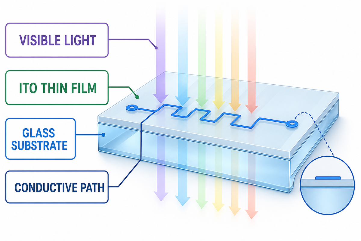
ITO coating adds a transparent conducting oxide layer to glass, so the same part can transmit visible light and carry an electrical function. In buyer language, the coating turns optical glass into conductive glass for touch panels, displays, heaters, sensors, EMI shielding, and control-panel surfaces.
Indium tin oxide coatings are valued because the film can combine optical transmission with useful conductivity. That balance is the reason ITO appears in display glass, touch screen glass, transparent heaters, smart home devices, medical equipment panels, and industrial HMI covers. Saiwei’s related touch screen glass work gives that use case a clear product context.
There is still a tradeoff. A conductive ITO film is not just a clear varnish. It is a measured layer with sheet resistance, optical properties, adhesion, haze, reflection, coating-side direction, and handling constraints. If the project also needs anti-reflective, anti-glare, anti-fingerprint, printing, cutting, strengthening, or edge work, those downstream steps need to be planned around the conductive surface.
For a controlled RFQ, write the active area as a dimensioned zone and pair it with a target such as 30 ohms/sq at +/-20% over a 9-point map.
ITO-coated glass is sometimes compared with FTO glass, especially when heat stability or chemical exposure is part of the design review. Keep that comparison application-specific. An indium tin oxide film is usually selected for its electrical and optical properties in a defined stack, not because ITO or FTO is always better in every device.
ITO belongs to transparent conducting oxides, so the buying question is which deposition techniques fit the glass, quantity, and acceptance window. Magnetron sputtering is the practical focus here; chemical vapor deposition appears in broader thin-film literature, but most RFQs should define the required indium tin oxide film, indium tin oxide coatings, and conductive ITO film by electrical and optical properties, not by process name alone.
For adjacent surface-treatment decisions, review Saiwei’s glass coating types guide and AR vs AG vs AF coating guide. This article stays narrower: ITO deposition, resistance target, cost drivers, and RFQ decisions. Buyer searches such as ito glass coating, ito sheet resistance, ito coated glass price, and ito coated glass suppliers all need the same quote boundary.
Magnetron Sputtering Workflow for ITO Coated Glass
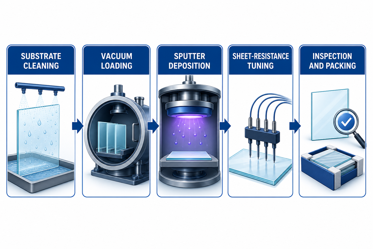
Magnetron sputtering is a common route for ITO coated glass because it can form a controlled thin film from an ITO target under vacuum. The process is sensitive to cleaning, plasma conditions, gas flow, power, substrate temperature, deposition time, and post-coating heat treatment.
A practical sputtering process starts before the chamber door closes. The substrate is cut or supplied in the required size, cleaned to remove particles and residues, checked for surface defects, and loaded into fixtures. Handling matters because a small contaminant can become a visible defect, a local resistance change, or a yield loss on a coated part.
Inside the chamber, argon plasma ejects material from the ITO target and deposits it on the glass substrate. Oxygen flow, pressure, power, target condition, throw distance, and movement across the coating zone affect film growth. Peer-reviewed ITO sputtering studies show that oxygen flow and related deposition conditions can change sheet resistance, resistivity, and transmittance together.
The post-deposition steps depend on the part. Some projects require anneal treatment to shift conductivity or optical performance. Others need masking, patterning, contact pads, bus bars, edge deletion, lamination, screen printing, or another coating stack. If the glass also needs AR or AF treatment, the stack order and coating-side direction should be settled before samples are made. Saiwei’s anti-reflective coating guide explains the separate optical-coating side of that conversation.
| Process stage type | What the supplier controls | Why it changes quote risk |
|---|---|---|
| 1. Substrate intake | Glass type, thickness, size, edge condition, coating side, flatness. | Large, thin, or tight-cosmetic glass can reduce yield and slow handling. |
| 2. Cleaning | Particle removal, detergent or DI rinse, drying, surface check. | Cleaning failures can turn into pinholes, visible spots, or local resistance drift. |
| 3. Loading and fixture | Carrier, shadow mask, active area, edge exclusion, orientation. | Custom masks and low-volume fixtures add setup time. |
| 4. Vacuum pump-down | Chamber pressure, leak check, outgassing control. | Dirty or high-outgas loads extend cycle time and can hurt repeatability. |
| 5. Plasma sputter | Power, gas flow, pressure, target condition, deposition time. | This is where conductivity, transmittance, thickness, and uniform coating goals meet. |
| 6. Optional anneal | Temperature, dwell time, cooling path, glass limit. | Heat-sensitive glass, prints, or laminated parts narrow the route. |
| 7. Pattern or contact | Masking, etching/removal, bus bars, terminal areas. | Patterned ITO takes more setup and inspection than blanket coating. |
| 8. QC measurement | Sheet resistance map, optical check, visual inspection, sample record. | A multi-point map and tight acceptance band cost more than a nominal check. |
| 9. Packing and release | Surface protection, coating-side label, clean packing, lot trace. | Handling scratches or wrong-side assembly can waste finished panels. |
9-Variable Sheet-Resistance Tuning Map: Thickness, Oxygen, and Annealing
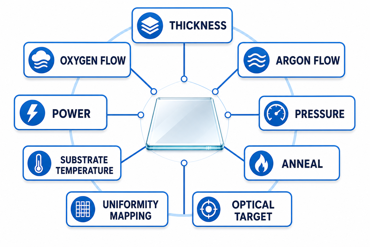
Sheet resistance, written in ohms/sq, is the buyer’s main electrical shorthand for an ITO thin film. It is tuned through film thickness, oxygen balance, gas flow, power, temperature, anneal route, and uniformity control, while transmittance and appearance still have to remain inside the project window.
Lower sheet resistance often means a thicker or more conductive film, but it should not be specified alone. A common assumption is that the lowest ohms/sq is automatically the best buying target. That is not always true: the cheapest ITO coating is rarely the best choice if it misses optical acceptance, contact design, or uniformity mapping. The right target is a window, not a single heroic number.
Current research examples show why the numbers need context. One MDPI ITO sputtering study reports oxygen-flow examples around 63 ohms/sq with 79.2% transmittance at 3 sccm oxygen and around 77 ohms/sq with 80.8% transmittance at 4 sccm oxygen. An Optica 2026 ultrathin-film study reports a 4.0 nm film example at 156.6 ohms/sq and around 97.3% normalized transmittance under its stated conditions. These are study examples, not universal production guarantees.
Saiwei’s first-party manufacturing profile states that its ITO coated glass can be customized from 3-800 ohms/sq. Treat that as a capability range for RFQ discussion. The final target should still include substrate, size, tolerance, optical target, measurement method, and drawing-level acceptance details. For company context, see the Saiwei Glass manufacturing profile.
| Tuning variable | Electrical effect to discuss | Optical or production check | RFQ wording |
|---|---|---|---|
| Film thickness | Can lower sheet resistance as conductive path increases. | Can shift transmittance, color, haze, and stress. | State resistance target plus optical target, not thickness alone. |
| Oxygen flow | Changes carrier behavior, resistivity, and repeatability. | Needs transmittance basis and process control record. | Ask for the supplier’s tested range and inspection plan. |
| Argon flow and pressure | Affects plasma stability and deposition process repeatability. | Can affect uniform coating across the panel. | Request tolerance by active area, not one center point. |
| Sputter power | Changes deposition rate and film density. | Can change heat load and visible defects. | Let the supplier tune power to the target window. |
| Substrate temperature | Can influence conductivity and crystallinity. | Glass, print, or laminate limits may cap temperature. | Declare any heat-sensitive downstream process. |
| Anneal step | May reduce resistivity under controlled conditions. | Needs time, temperature, and glass compatibility. | Say whether anneal is allowed after coating. |
| Target condition | Target age and conditioning can affect run stability. | Can influence lot consistency and yield. | Ask for lot traceability on production orders. |
| Panel movement | Uniformity depends on path through the coating zone. | Large panels need edge-to-center checks. | Specify map points or sampling plan. |
| Patterning | Local resistance can depend on trace geometry. | Edges, isolation gaps, and contacts need inspection. | Attach CAD drawings and active-area rules. |
11-Driver ITO Cost Driver Matrix
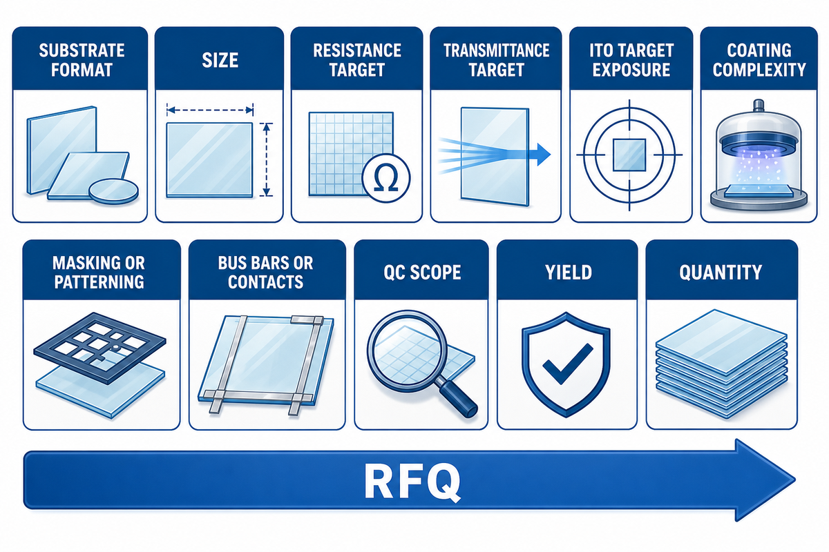
The ITO Cost Driver Matrix begins with material exposure but doesn’t end there. Indium market data, ITO targets, substrate area, coating time, masking, patterning, yield, and scope of QC also shape the quote, so a supplier needs the full job boundary before pricing.
The official USGS 2026 Indium mineral commodity summary gives raw indium supply context: the estimated annual average U.S. warehouse price in 2025 was $390 per kilogram, 11% more than in 2024; U.S. net import reliance was 100%; and China accounted for 70% of world refinery production. Those figures support material-exposure awareness, not a finished ITO coating price.
Target economics also need care. ITO target utilization isn’t the same as deposited film on sellable glass. Target reclaim, recycling, chamber geometry, run size, and scrap rate can all mediate the raw-material signal. A quote that hides those process factors behind a square-meter number is hard to compare.
| Cost driver | What changes | Buyer question | Quote effect |
|---|---|---|---|
| Substrate material | Soda-lime, aluminosilicate, borosilicate, tempered or strengthened glass. | Does the glass survive cleaning, vacuum, and anneal conditions? | Changes handling route and process limits. |
| Substrate size | Small coupons, display covers, large panels, odd shapes. | Will the chamber and fixture handle this format efficiently? | Changes batch loading and yield exposure. |
| Resistance target | 3-800 ohms/sq range discussions need tolerance and active area. | Is the target low, high, or tight across the panel? | Can lengthen tuning, deposition, or inspection. |
| Transmittance target | Visible light transmission, wavelength range, haze, reflection. | What measurement basis and wavelength range are required? | Can narrow process and coating-stack options. |
| ITO target exposure | Target material, run duration, reclaim or recycling practice. | Is this prototype, repeat lot, or high-volume program? | Raw material signal is mediated by utilization and recovery. |
| Masking or patterning | Blanket coating, active windows, traces, isolation zones. | Is a drawing available with tolerance and edge exclusion? | Adds setup, inspection, and scrap risk. |
| Bus bars and contacts | Conductive paths, terminal areas, silver paste, bonding interface. | How will the coated glass connect to the device? | May add printing, curing, and electrical testing. |
| QC scope | Point check, sheet-resistance map, optical report, cosmetic grade. | Which acceptance method decides pass or fail? | More measurement points add time but reduce ambiguity. |
| Yield and cosmetics | Scratch class, pinholes, stains, edge chips, clean-room packing. | What defects are allowed in active and border areas? | Tighter cosmetic rules raise rejection exposure. |
| Quantity and forecast | Samples, pilot lots, annual demand, reorder rhythm. | Can setup be amortized across repeat production? | Unit economics change between sample and volume. |
| Lead time | Urgent sample, standard batch, fixed production slot. | Does the due date allow tuning and confirmation samples? | Rush timing can reduce scheduling flexibility. |
9-Row Process-to-Price Decision Table
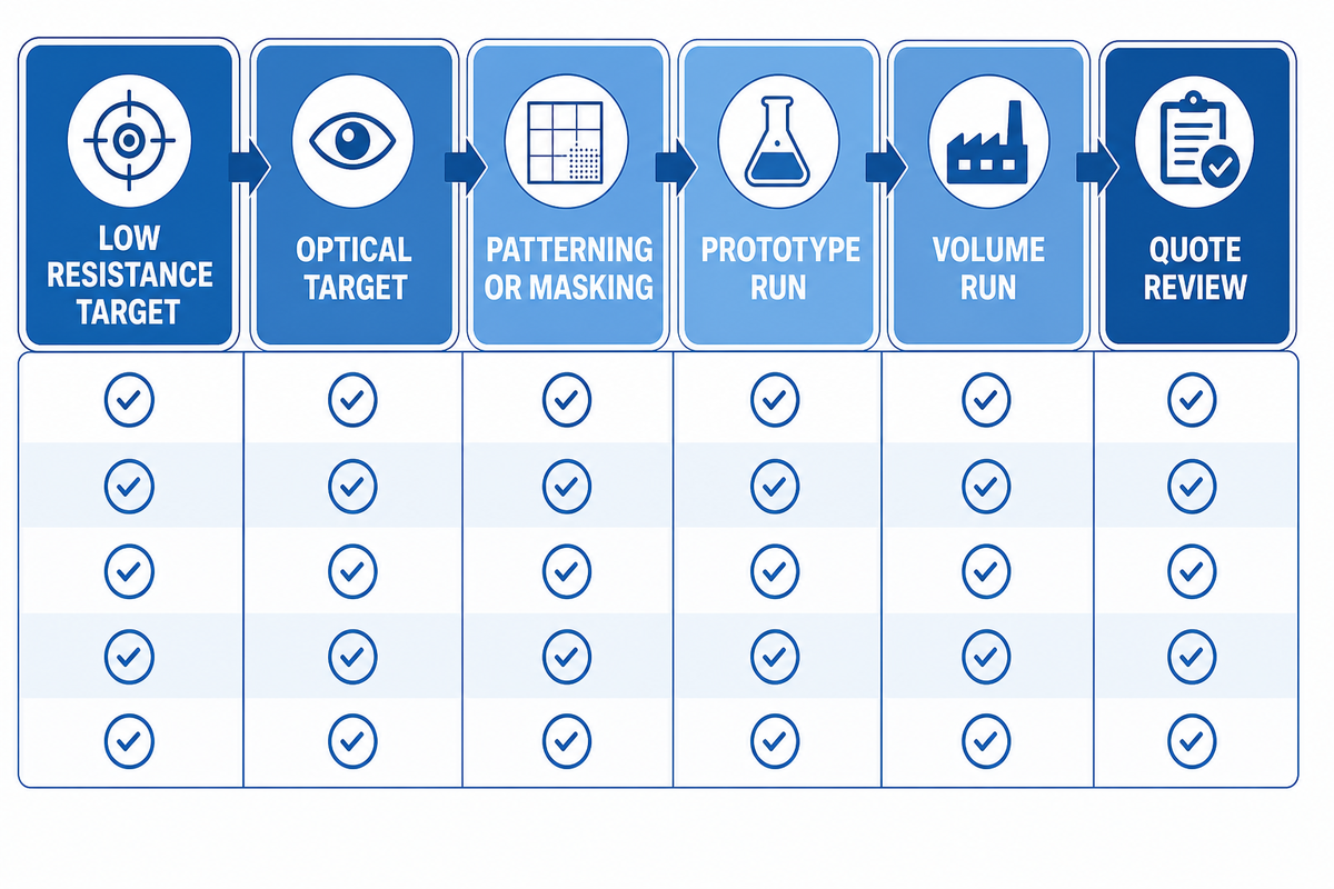
The Process-to-Price Decision Table turns technical requirements into buying choices. A buyer can reduce quote friction by separating must-have limits from nice-to-have preferences, then letting the coating supplier choose the sputtering process window that meets the electrical and optical targets.
Start with the application. A touch sensor, transparent heater, EMI-shielding panel, medical display cover, and laboratory electrode don’t need the same resistance, transmittance, or cosmetic grade. Chasing the lowest possible sheet resistance can be wasteful when the circuit only needs a higher resistance band and better optical clarity.
One counter-intuitive point is worth making early: film thickness and sheet resistance shouldn’t be specified as if they were independent purchase items. Research on ITO thin films shows that thickness, transparency and conductivity can move together in ways that depend on process conditions. If a buyer writes both a thickness and an ohms/sq target without a measurement hierarchy, the supplier may not know which one governs acceptance.
| Buyer decision | Lower-risk wording | Riskier wording | Why it matters |
|---|---|---|---|
| Resistance | Target 30 ohms/sq, +/-20%, measured at 9 points in active area. | Make it as conductive as possible. | The first version defines acceptance; the second invites over-processing. |
| Optical target | State visible transmittance basis and any haze or reflection limits. | High transparency required. | Measurement basis affects comparison across suppliers. |
| Coating area | Attach drawing with active area, border, coating side, and edge exclusion. | Coat the whole sheet unless not needed. | Blanket coating may waste target material or create assembly problems. |
| Patterning | Provide CAD lines, isolation width, and test points. | Patterned ITO, details later. | Pattern setup changes lead time and inspection. |
| Contacts | Name bus bar material, location, width, curing limits, and resistance check. | Add contacts if needed. | The electrical interface can become the real failure point. |
| Surface stack | Say whether AR, AF, AG, printing, strengthening, or lamination follows ITO. | ITO now, other coatings later. | Stack order and heat limits can block late changes. |
| Sampling | Request sample quantity, test report, and acceptance plan. | Send a few pieces first. | Unclear samples do not predict volume yield. |
| Volume | Provide pilot lot and annual forecast separately. | Quote samples and mass production in one line. | Setup and yield cost are allocated differently. |
| Delivery | Give desired ship date and approval deadline. | As soon as possible. | Tight timing may limit test repeats and process tuning. |
9-Field QC and RFQ Spec Stack
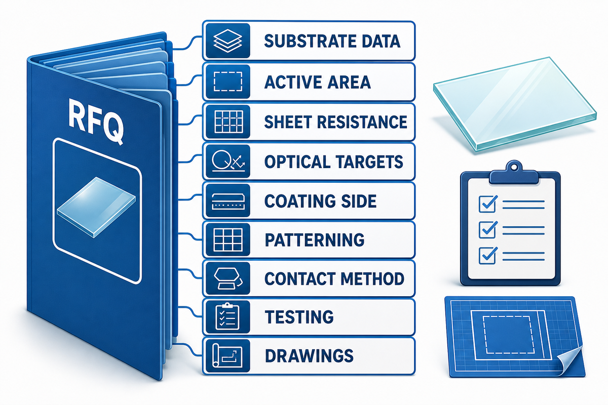
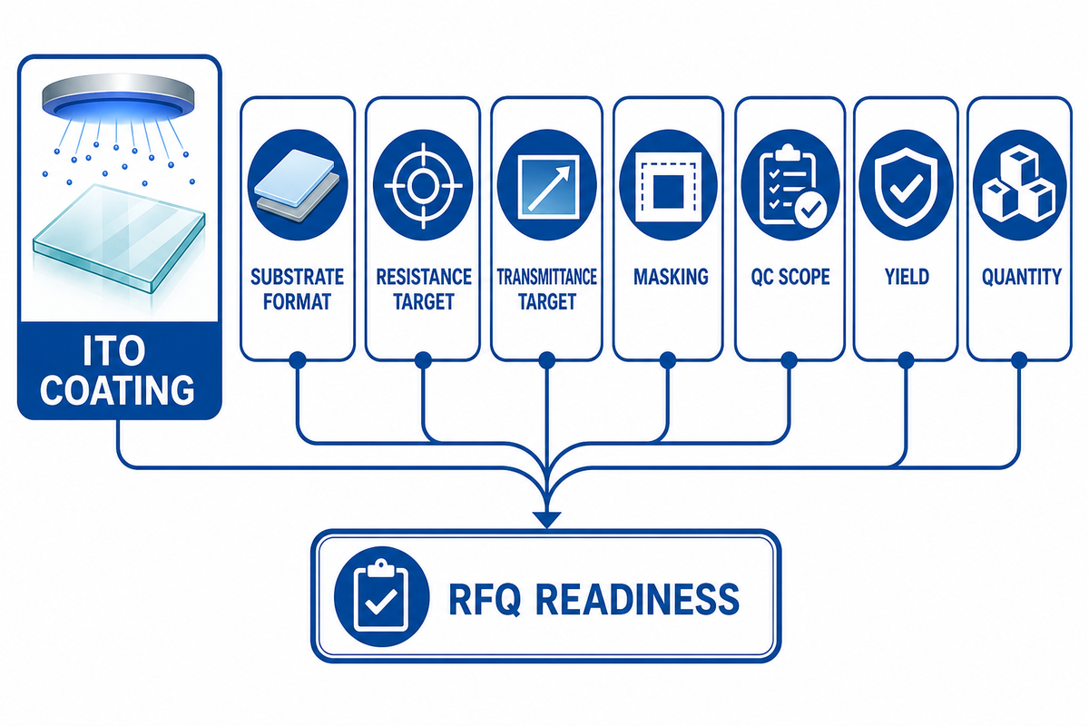
The RFQ Spec Stack is the short checklist that makes an ITO quote comparable. It should define the glass, active area, sheet resistance, tolerance, optical target, coating side, patterning, contacts, sample plan, volume forecast, and test method before price is negotiated.
Sheet-resistance measurement is usually discussed through four-point-probe methods for thin conductive films. NIST measurement work and ASTM practice language support that general QC concept, while still leaving the actual acceptance plan to the drawing, supplier method, and project contract. For large panels, ask for multi-location measurement rather than relying on a single center reading.
Optical measurement needs the same discipline. ISO 15368:2021 covers spectral reflectance and transmittance measurement rules in optics and photonics, including the difference between regular and diffuse transmittance contexts. So a public number such as 90% or 97.3% is not enough unless the wavelength range, substrate, and measurement basis are stated.
| RFQ field | Minimum data to send | Why it prevents quote drift |
|---|---|---|
| Glass substrate | Material, thickness, size, strengthening state, edge finish. | Defines thermal and handling limits. |
| Active area | Coated window, border, mask, edge deletion, no-coat zone. | Separates useful coating from nonfunctional area. |
| Sheet resistance | Target ohms/sq, tolerance, map points, acceptance method. | Stops one nominal number from hiding a broad spread. |
| Optical target | Transmittance range, wavelength basis, haze, reflection, color limit. | Makes optical comparison fair. |
| Coating side | Side A or Side B, assembly direction, touch or protected face. | Prevents wrong-side assembly and handling damage. |
| Patterning | CAD file, tolerance, isolation gaps, pads, lead-out zone. | Lets the supplier estimate masking, etch, and inspection work. |
| Contacts | Bus bar material, terminal layout, cure limit, contact resistance target. | Connects the film to the electrical design. |
| Environmental checks | Heat, humidity, abrasion, cleaning, salt mist, or application-specific tests. | Moves durability from guesswork into acceptance evidence. |
| Order plan | Sample count, pilot lot, volume forecast, packaging, delivery date. | Separates one-time setup from repeat-production assumptions. |
When to Request ITO Coating Services
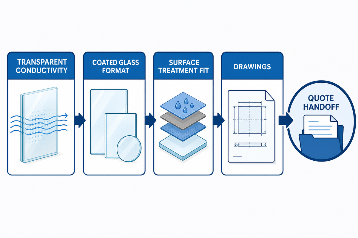
Request ITO coating services when the glass must be both optically usable and electrically functional, and when the quote can be tied to a drawing, resistance window, optical target, and inspection method. Saiwei can discuss custom resistance targets, coating stack order, and production route after those inputs are clear.
For commercial discussion, use Saiwei’s ITO coating services page as the handoff. The same page sits beside AR and AF surface-treatment capability, which matters when final glass needs transparent conductivity plus anti-reflective or anti-fingerprint performance.
Saiwei Glass states a precision glass processing background with custom ITO coated glass resistance from 3-800 ohms/sq, 1M+ annual capacity, 50+ technicians, and 100+ automated equipment. Those are useful first-party scale signals. The right engineering next step is still a controlled RFQ: drawing, sample target, volume forecast, and test plan.
Attach substrate size, target ohms/sq, optical requirement, coating side, quantity, drawings, and any AR/AF/AG or printing steps planned after ITO.
FAQ
What is the process of ITO coating glass?
ITO coating glass is made by preparing the substrate, cleaning the surface, loading it into a vacuum system, sputtering indium tin oxide from a target, controlling film growth, and then checking sheet resistance and optical performance. Many production routes use magnetron sputtering, although other deposition techniques such as evaporation or chemical vapor deposition appear in technical literature. Production release then depends on inspection records, coating-side marking, packing protection, and any downstream AR, AF, AG, printing, or lamination step. For prototypes, the process should also include a sample signoff because one accepted coupon rarely proves yield on a larger display cover or industrial panel. On shaped parts, coated-side handling, edge deletion, and protected contact areas should be reviewed before the lot enters the vacuum chamber.
Why does lower sheet resistance usually cost more?
Achieving lower ohms/sq typically means longer deposition time, greater sputtering-target exposure, stricter control of process parameters, narrower optical trade-offs, and more process checks. Customers should carefully specify their performance expectations rather than assuming that lower electrical resistance is inherently better, and they should identify the target value and test method that will confirm a suitable device.
Can sheet resistance and optical transmittance be tuned at the same time?
Yes, but they should be tuned as a pair and checked on the same coated-glass sample. A thicker or more conductive ITO film may lower resistance while changing visible transmittance, reflection, haze, or color. A thinner film may protect transparency but raise resistance. Your RFQ should define both targets and the measurement basis, including wavelength, tolerance band, and acceptance priority.
What should I prepare before asking for an ITO coating quote?
Send the substrate type, thickness, full external dimensions, functional dimensions of the display area, surface(s) to be coated, desired Ohms resistance and tolerance, visible light transmittance or other optical requirements, mask layout file, physical device interconnections required, sample quantity, anticipated production volume, cosmetic standards, and project timeline. If future process steps like AR coatings, anti-fingerprint treatments, surface etching (AG), printing or laminations are planned, provide the sequence of operations to us prior to sample coating. Submit drawings illustrating no-coating borders, electrical contact pads, display regions, or reference marks.
References & Sources
- U.S. Geological Survey: Indium Statistics and Information
- U.S. Geological Survey: 2026 Indium Mineral Commodity Summary
- U.S. Geological Survey: Mineral Commodity Summaries 2026
- MDPI Coatings: Indium Tin Oxide Thin Film Deposition by Magnetron Sputtering at Room Temperature
- Optica: Influence of process parameters on sheet resistance and transmittance of ultrathin ITO films
- NIST: Four-point probe sheet-resistance measurement publication
- ANSI Webstore: ASTM F1711-96 sheet resistance practice listing
- ISO: ISO 15368:2021 optics and photonics measurement standard page
- CDC/NIOSH: Use of and Occupational Exposure to Indium in the United States
- Indium Corporation: ITO sputtering target reclaim and recycling
- Photonics: Optical coating materials and deposition technology