Póngase en contacto con Saiweiglass


ITO Glass Explained: Properties, Conductivity & Industrial Applications


Contenidos
mostrar
Industrial conductive glass guide
ITO glass is a glass substrate coated with indium tin oxide, a transparent conductive oxide that lets light pass while carrying electrical current across the glass surface. It’s used when engineers need a transparent electrode for touchscreens, displays, sensors, heaters, solar cell research, and other optoelectronic assemblies.
What Is ITO Glass?
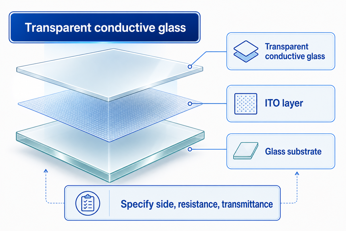
ITO glass is transparent conductive glass made by depositing a thin layer of indium tin oxide on a glass substrate. The coating behaves like an electrical conductor, while the glass keep the optical clarity, stiffness, and dimensional stability needed in displays, touch panels, transparent heaters, laboratory electrodes, and thin-film photovoltaic research.
In material terms, indium tin oxide is a tin-doped indium oxide. It belongs to the transparent conducting oxide family, often shortened to TCO. The practical value is the unusual combination of transparency and conductivity: the surface can transmit visible light while serving as an electrode. Public technical reviews describe ITO as a widely used TCO in flat panel displays, touchscreens, solar cells, antireflection coatings, and smart windows.[1]
That combination is why ITO coated glass is different from ordinary soda-lime, aluminosilicate, low iron glass, or chemically strengthened cover glass. Plain glass can protect a display or sensor; ITO coated glass can also become part of the circuit. The coating is usually invisible to the end user, but it controls touch response, transparent electrode behavior, electrical resistance, and the interaction between display stack, controller, adhesive, and cover glass.
For buyers, the label “ITO glass” is only the starting point. A usable drawing or purchase specification should define substrate type, thickness, coating side, sheet resistance, transmittance, ITO film thickness in nm, patterning requirements, edge contact area, inspection method, packing, and downstream processing limits. Without those details, two parts can both be called ITO coated glass while behaving differently in a finished module.
ITO Glass at a Glance
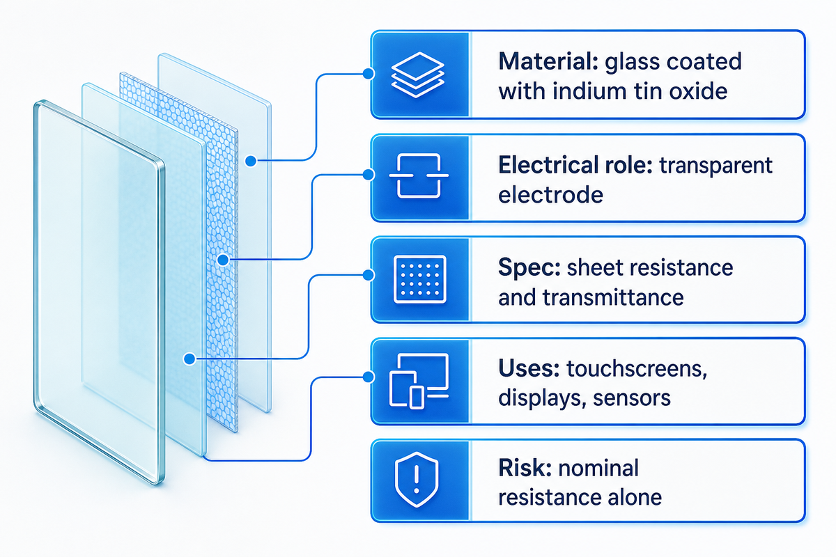
| Material | A glass sheet, glass plate, or glass slides coated with indium tin oxide. |
|---|---|
| Electrical role | Transparent electrode or electrically conductive layer. |
| Common spec | Sheet resistance in ohms/sq, plus optical transmittance and coating uniformity. |
| Typical uses | Touchscreens, LCD and OLED displays, solar cell research, sensors, smart windows, transparent heaters, and EMI shielding.[1] |
| Main risk | Choosing only by price or nominal resistance without matching the stack, contact design, and processing route. |
How Does ITO Glass Conductivity Work?
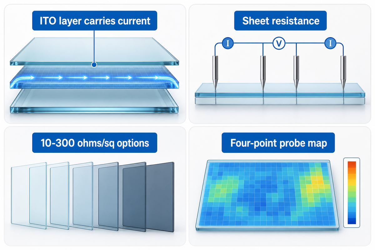
ITO glass conductivity is usually specified as sheet resistance, measured in ohms per square, because current travels through a very thin conductive layer rather than through the glass itself. Lower sheet resistance can improve current spreading, but it isn’t a standalone performance rating. Geometry, contact design, coating uniformity, pattern visibility, optical stack, and measurement method can change the actual module result.
The underlying glass is an insulator. The ITO layer on the surface carries the current. Engineers often describe that layer as a transparent conductive film, an ITO thin film, or a transparent electrode. One review of transparent conducting oxides reports high optical transparency above 80 percent and high conductivity near 10^4 ohm^-1 cm^-1 for ITO, while also noting trade-offs around indium cost, byproduct supply, surface energy, and stability.[2]
Sheet resistance is the most useful day-to-day specification because it lets designers compare coatings across different shapes. Common touch or display projects may ask for values such as 10, 30, 50, 100, or 300 ohms/sq, depending on sensor geometry and controller needs. Saiwei’s ITO touch screen glass capability page lists ITO resistance options from 10-300 ohms/sq, which is a practical range for custom touch panel discussions.
Measurement language matters. BYU’s cleanroom guide explains the relationship between measured resistance and sheet resistance as R = Rs(L/W), and notes that two-point readings can include contact resistance.[10] NIST describes sheet resistance mapping systems that use four-point probe measurement to check substrates and films across an area, which is why a production drawing should define the test method, sampling points, and acceptance map, not only one nominal ohms/sq number.[11]
The counterintuitive point is that “lower is always better” isn’t a reliable rule, but the trade-off is process-dependent rather than a simple inverse relationship. Lower-resistance coating can require a thicker or more heavily optimized conductive film. That can shift optical transmission, haze, color neutrality, stress, brittleness, patterning behavior, and cost. In one OSTI-indexed annealing study, rapid thermal annealing at 600 C produced both lower resistivity and 92 percent transmittance under its specific process conditions.[9] In flexible devices, thick ITO can still become a failure point, and technical coverage of flexible touch use has highlighted brittleness as a limitation when ITO is forced outside its best mechanical window.[3]
Practical specifications should therefore pair sheet resistance with transmittance, haze, coating side, busbar/contact method, environmental exposure, laser or chemical etch plan, downstream bonding temperature, and visual inspection of patterned regions. If the conductive glass will be laminated under vidrio de cubierta personalizado, the adhesive, ink border, sensor pitch, shield layer, and any low-reflection or index-matching design also need to be included in the stack review.
Key Properties Buyers Should Compare
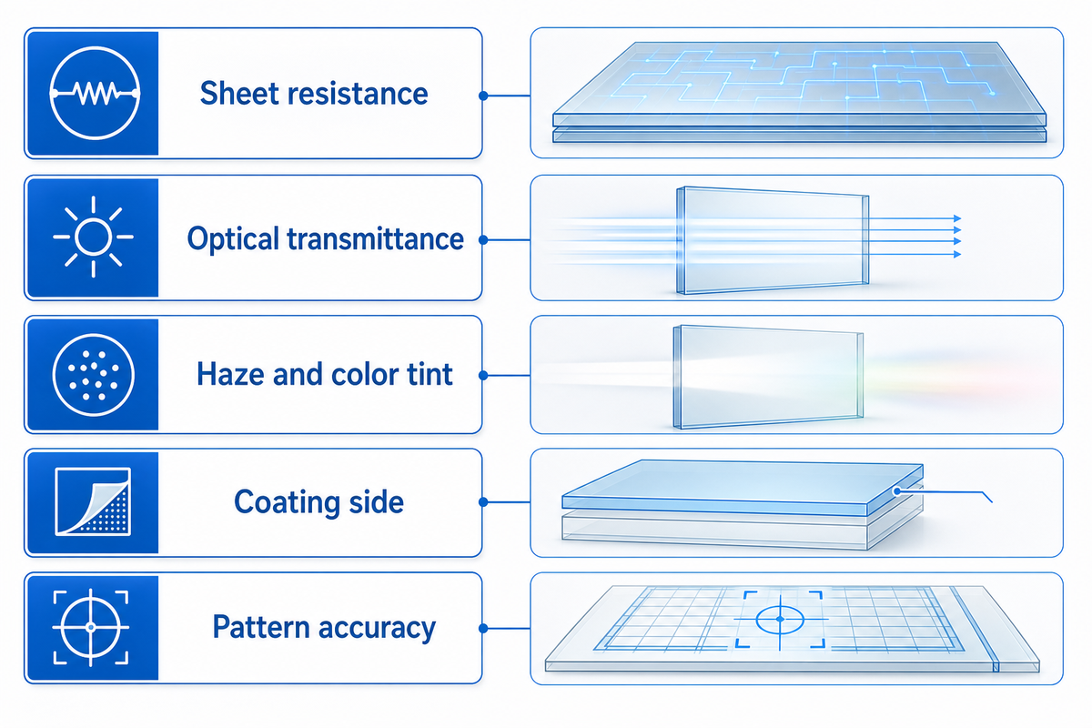
ITO glass substrates should be compared as an electrical and optical component, not only as a piece of coated glass. The basic property set includes sheet resistance, resistivity, optical transmittance, haze, coating uniformity, substrate thickness, thermal history, edge quality, surface cleanliness, and pattern accuracy.
The practical properties of ITO depend on the coating recipe and finished stack: a highly conductive film near 100 ohms per square can be right for one sensor or heater layout and wrong for another if transparency, uniformity, contacts, and module noise aren’t controlled together.
Sheet resistance controls current spreading. Transmitancia controls how much visible light passes through the stack. Haze and color tint affect display readability. Coating side matters because the conductive surface must face the electrode, adhesive, or touch sensor structure specified by the design. Surface of ITO cleanliness matters because residue can weaken bonding, cause nonuniform contact resistance, or create cosmetic defects under a display. For optical acceptance, avoid a single vague “transparency” value. ISO 15368:2021 covers spectral regular transmittance and reflectance of coated or uncoated plane optical components and explicitly separates those measurements from diffuse transmittance and diffuse reflectance.[14] For patterned touch electrodes, optical difference between conducting and insulating regions can also create visible artifacts; an Optics Express study on transparent electrodes discusses low-reflection and oxide-metal-oxide strategies to reduce pattern visibility in sensor/display stacks.[12] A Nature/Springer study on on-screen fingerprint sensors shows why this matters: even ITO electrodes around 10 ohms/sq and 94 percent visible transmittance can still degrade display quality when periodic sensor patterns interfere with display pixel arrays, so pitch and rotation need validation for display-over-sensor designs.[21]
Visible transmittance is also not an intrinsic constant of “ITO glass.” One PubMed-indexed sputtering and annealing study reported that an as-grown 110 nm ITO film showed 34.2 percent transmittance at 550 nm and 9.2 x 10^-4 ohm cm resistivity, while nitrogen annealing at 850 C for 1 minute produced 97.3 percent transmittance and 1.3 x 10^-4 ohm cm resistivity.[17] If the project cares about infrared, terahertz, thermal radiation, or sensor wavelengths outside a normal display window, specify the wavelength band separately. Coatings published a 2024 paper on ITO thin films with visible-window values over 400-800 nm and separate 0.2-1.0 THz transmittance values that changed with rapid thermal annealing, mobility, and carrier concentration.[19]
Substrate choice also changes the outcome. Standard ITO on glass is rigid and dimensionally stable, but substrate chemistry matters when annealing is involved. Research in Thin Solid Films on ITO over soda-lime glass reports that sodium ions can diffuse from the glass into ITO during annealing, increasing resistivity and structural defects, while SiO2 or Al2O3 barrier layers inhibit that diffusion.[23] ITO on quartz can support higher thermal or optical demands. ITO on PET substrates or polymer substrates can support flexible layouts, but it changes scratch resistance, thermal limits, and bend durability. FTO glass, AZO as a transparent conductive oxide based on aluminum-doped zinc oxide, and indium zinc oxide may be better in some high-temperature, cost-sensitive, or alternative TCO projects. ITO and FTO should be compared by process temperature, chemical durability, optical target, and electrical design, not by one headline value.
For touch display assemblies, the property conversation should include the whole stack: ITO layer, cover glass, printed decoration, anti-reflective or AR coating, anti-fingerprint or AF coating, optical bonding, controller sensitivity, and enclosure sealing. Saiwei’s AR and AF coating capability is relevant when the transparent conductive glass also needs better outdoor readability, fingerprint resistance, or cleaning performance.
| Use case | Sheet resistance direction | Key optical concern | Specification risk | Buyer action |
|---|---|---|---|---|
| Projected capacitive touch panel | Low to medium | Display clarity and low haze | Controller mismatch | Confirm sensor pitch, trace layout, and controller window. |
| Resistive touch panel | Application-specific | Uniform response | Spacer and contact wear | Define activation force and durability test. |
| Transparent heater | Lower resistance often needed | Thermal uniformity without visible tint | Hot spots at busbars | Model voltage, busbar width, and edge contact. |
| Solar cell research electrode | Low resistance with high light entry | Spectral transmittance | Chemical incompatibility | Check process temperature, etchant, and cleaning chemistry. |
| OLED or LCD display stack | Low and uniform | Color neutrality | Mura or nonuniform contact | Specify coating uniformity and inspection mapping. |
| Smart windows | Equilibrado | Large-area haze | Edge voltage drop | Review part size, busbar plan, and environmental cycling. |
| Laboratory glass slides | Specified by experiment | Clean surface and microscopy clarity | Wrong coating side | Mark coating side and packaging orientation. |
| EMI shielding window | Lower resistance favored | Transmission loss | Poor grounding | Define grounding path, coating overlap, and gasket design. |
| Industrial HMI cover stack | Controller-driven | Outdoor readability | Ink, coating, and adhesive conflict | Prototype the full stack before tooling. |
| Thin display cover assembly | Medium to low | Flatness and edge strength | Breakage during lamination | Confirm thickness, edge finishing, and chemical strengthening. |
How Is ITO Coating Glass Made?
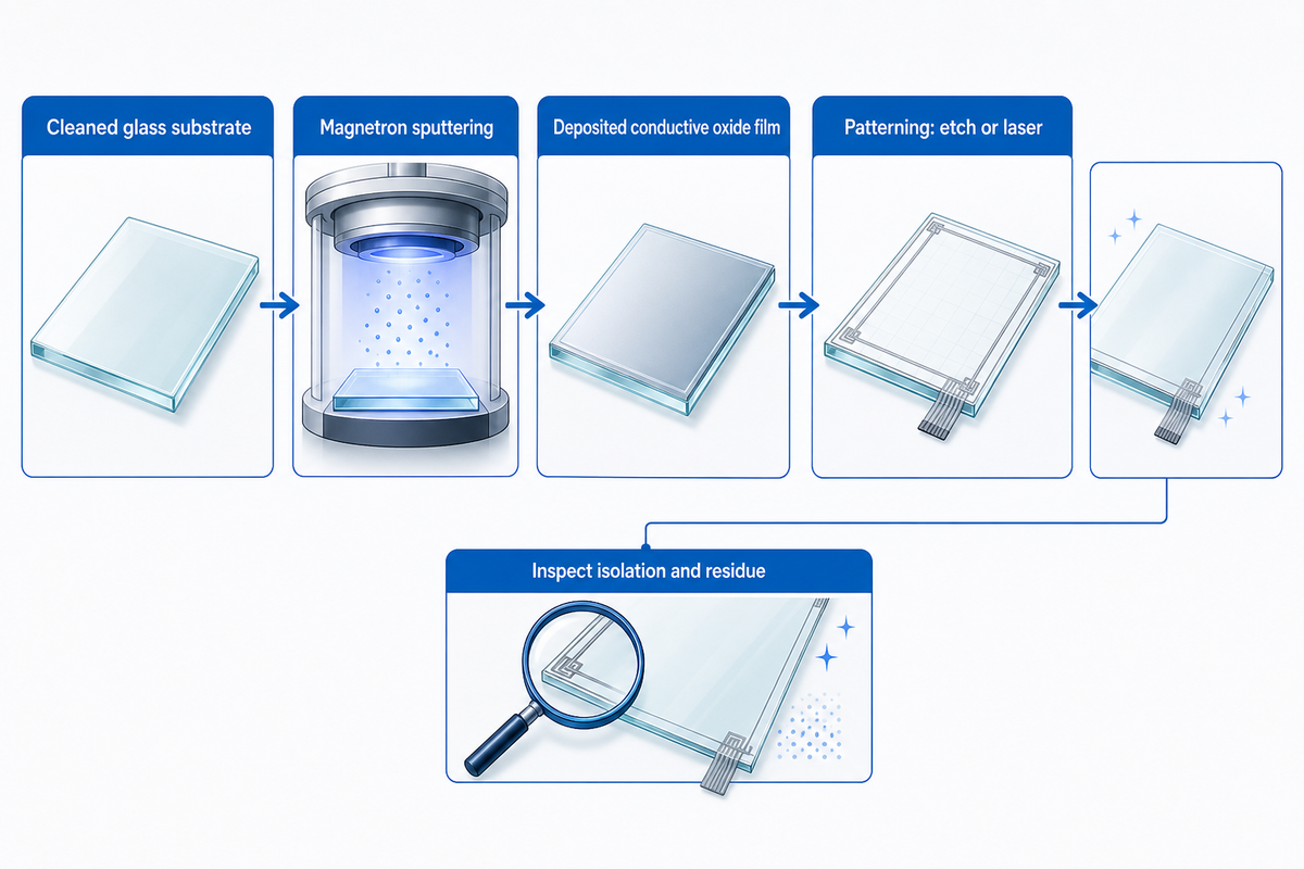
ITO coating glass is made by depositing a thin conductive oxide film onto a cleaned glass substrate, then annealing, patterning, cutting, cleaning, and inspecting it according to the application. Common deposition routes include magnetron sputtering, RF or DC sputter deposition, vapor deposition, pulsed laser deposition, sol-gel, and other thin-film fabrication methods.
For many industrial glass projects, magnetron sputtering is the main route because it can produce repeatable, uniform, transparent conductive layers on flat substrates. Technical reviews also discuss CVD, PLD, ALD, spin coating, inkjet printing, dip coating, nebulizer spray pyrolysis, and thermal evaporation. Each deposition method change coating density, oxygen vacancy behavior, substrate temperature, roughness, electrical and optical properties, and scale-up economics.[1]
After deposition, the ITO film may need patterning. In a touch panel, patterning divides the conductor into electrodes, channels, pads, and busbar areas. Patterned ITO glass can be produced through chemical etch, laser ablation, photolithography, or other precision processes. An OSTI record on high-temperature reactive ion etching describes ITO etching at 250 C with reported etch rates up to 435 angstroms/min under specific gas and plasma conditions, which illustrates how process-sensitive an ITO layer can be.[4]
Patterning quality isn’t only a cosmetic or line-width issue. A PMC article on laser-ablated ITO reports that ridges, nanoparticles, and residue can remain at ablated edges or surfaces and can contribute to open circuits, shorts between layers, adjacent-electrode shorts, and reduced device longevity.[18] For industrial touch glass, the drawing should therefore include electrical isolation checks, minimum line and gap rules, residue limits, edge morphology expectations, and test coupons after etching or laser ablation.
Patent literature also shows why ITO processing is treated as a controlled layer-forming problem rather than a simple coating add-on. Apple patent US8049862B2 describes forming crystalline ITO layers on substrates used in touch sensor panels, LCDs, and touchscreens.[5] That doesn’t mean every supplier uses the same route, but it does show how strongly ITO performance depends on deposition temperature, crystallinity, substrate limits, and subsequent assembly.
High-temperature glass processing should be reviewed before coating is locked. A PubMed-indexed Applied Optics study on ITO-coated automobile glass found that a surface-compression strengthening cycle with heating at 650 C for 5 minutes deteriorated electrical and optical properties of the ITO film, while a SiO2 barrier layer near 60 nm substantially reduced that loss.[15] For touch screen glass, that means the drawing should clarify whether strengthening, tempering, barrier layers, coating deposition, and patterning happen before or after each other.
When ITO glass will later be cut, drilled, printed, tempered, or bonded, the processing sequence matters. Coating damage, pinholes, scratches, edge chips, or wrong-side handling can turn a high-quality ITO glass sheet into a failed component. Production teams should also separate finished-product handling from dust-generating ITO manufacturing or maintenance tasks. NIOSH-linked research reports indium exposure above its recommended exposure limit during tasks such as sputter-target resurfacing and sputter-chamber cleaning; that evidence concerns airborne production exposure, not ordinary use of intact coated glass.[13] Para ultra-thin display glass, the process window is even tighter because handling strength, coating integrity, and lamination flatness interact.
What Is ITO Glass Used For?
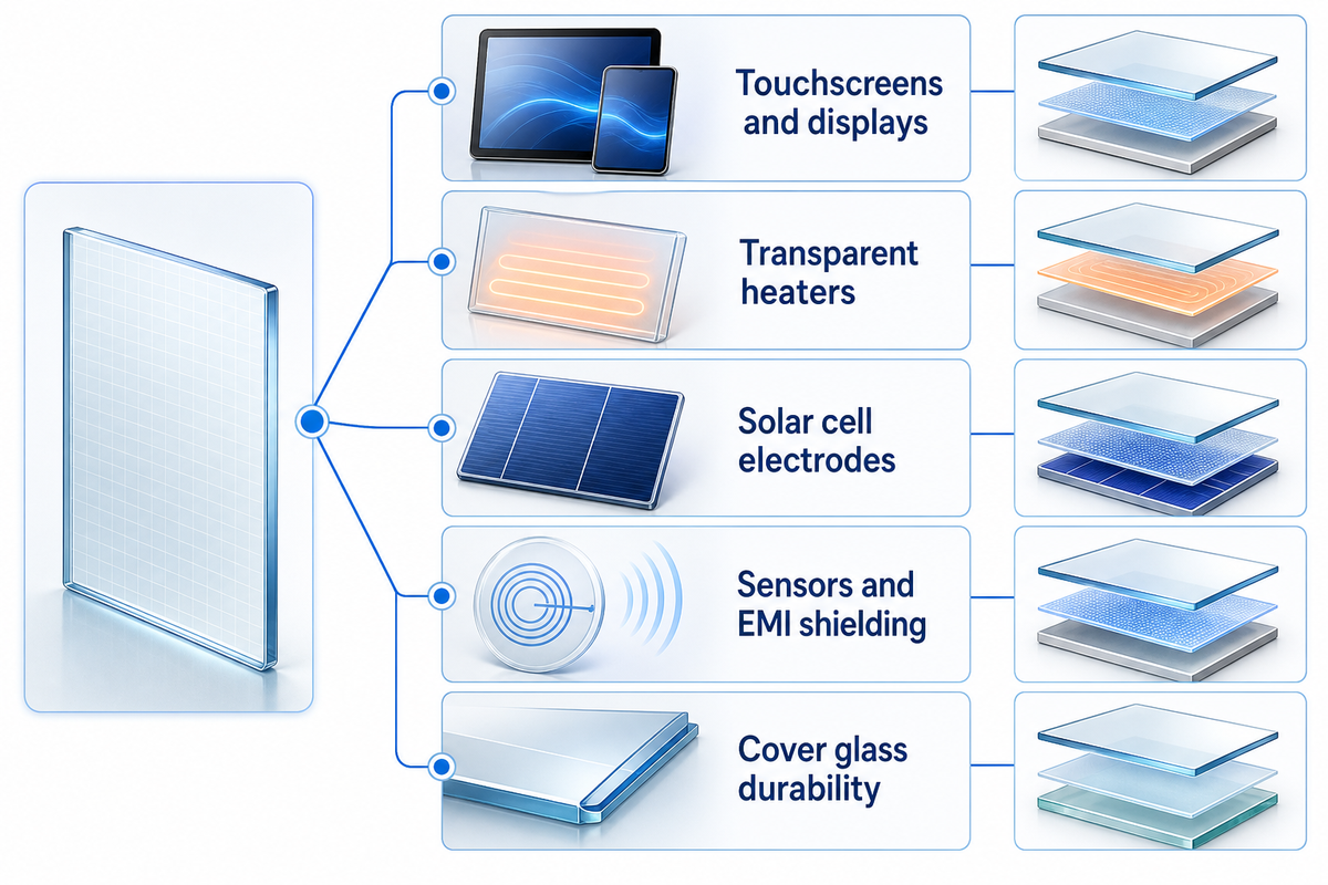
ITO glass is used wherever designers need a transparent conductive surface: touchscreens, flat-panel displays, OLED and LCD modules, transparent heaters, smart windows, solar cell electrodes, sensors, EMI shielding windows, microscopy slides, and research devices. It’s valuable because the conductor doesn’t block the user’s view through the glass.
USGS describes indium tin oxide as the most common use of indium and notes its role in flat-panel displays and touchscreens.[6] Transparent conducting film reviews expand the application set to solar cells, antireflection coatings, transparent p-n junction diodes, energy-efficient windows, and electronic devices.[1]
For industrial control panels, the value isn’t only electrical conductivity. Engineers also need a durable optical window that can survive cleaning, vibration, glove use, outdoor light, and enclosure assembly. In a kiosk or HMI system, the ITO conductive layer may sit below printed cover glass, adhesive, shielding, and a controller tuned for the panel’s size and layout. That’s why a component drawing should include the entire stack, not just the phrase “ITO coated”.
For solar cell and thin film solar research, ITO substrates work as transparent conductive electrodes that let light enter the active layer. Researchers may choose standard ITO, high-quality ITO, FTO, AZO, or another TCO depending on process temperature, chemistry, and band alignment. In organic light-emitting diodes and other semiconductor devices, the conductor, work function, surface roughness, and cleaning process can affect device performance. Reviews of TCO use in solar cells discuss work function, carrier mobility, and completed-stack behavior as performance variables, so a bench sheet-resistance value on glass shouldn’t be treated as a full device qualification by itself.[2] Scanning electron microscopy, four-point probe checks, and optical transmission tests may be used when the application is sensitive enough to justify lab verification.
For industrial and commercial touch assemblies, ITO glass connects naturally to Saiwei’s guía de selección de pantalla táctil industrial y POS and kiosk touch screen glass work. The ITO layer helps solve the sensing problem, while the cover glass, decoration, edge treatment, and coatings solve the usability and durability problem.
ITO Glass vs FTO, AZO, PET, and Plain Glass
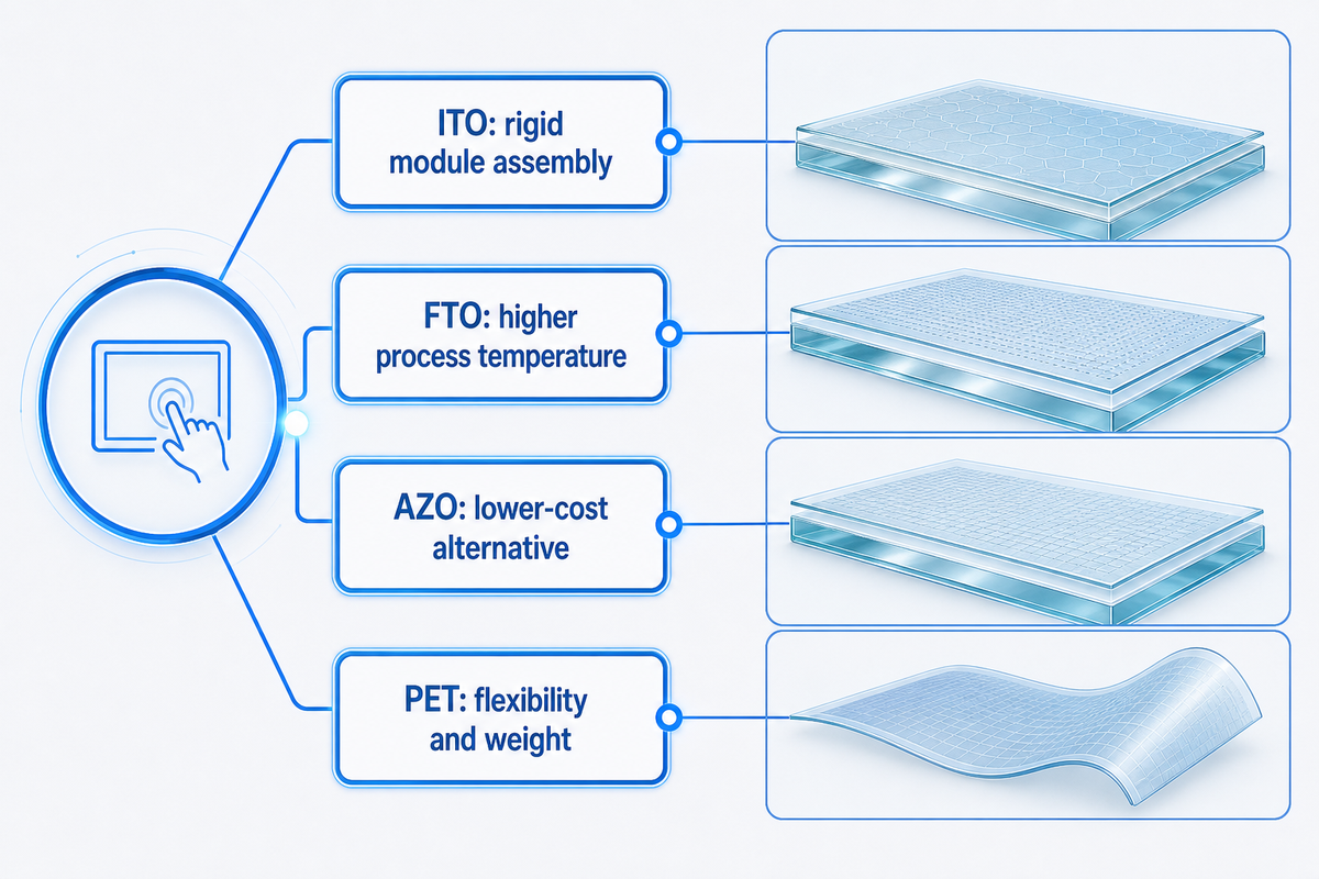
ITO is widely used, but it isn’t the only transparent conductive glass or film option. FTO glass uses fluorine-doped tin oxide and can be attractive where higher process temperatures or chemical durability matter. AZO uses aluminum-doped zinc oxide; zinc oxide based TCOs are often discussed as lower-cost alternatives, though humidity stability and electrical performance can be harder to manage. Indium zinc oxide and other TCOs may fit specialized display or optoelectronic uses.
PET substrates and polymer substrates are considered when flexibility or weight matters, but they introduce different scratch, temperature, and dimensional-stability constraints. Conducting polymer films, silver nanowires, graphene, and metal meshes can also appear in transparent conductive film discussions. IEEE Spectrum has covered ITO’s touchscreen role while also pointing to supply, cost, and alternative-material concerns.[7]
The practical comparison is straightforward: use glass-based ITO when optical transparency, flatness, dimensional stability, mature supply, and rigid module assembly are more important than flexing. Consider alternatives when high-temperature processing, very large-area cost, bend radius, indium supply risk, or unusual chemistry dominates the design. For cover structures that need better color rendering, low iron glass may also be part of the optical stack; Saiwei’s low iron glass material page is a useful related reference.
Selection Framework: Match Sheet Resistance to Application
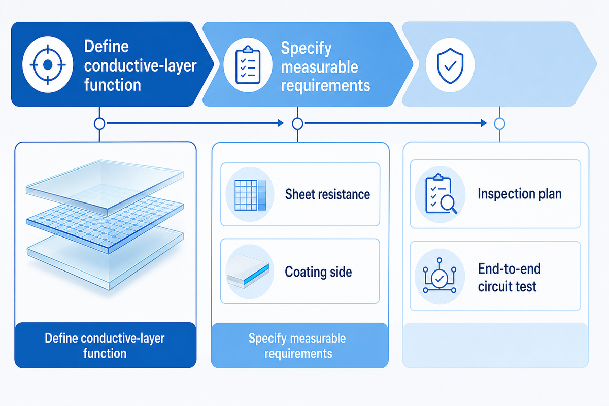
Start by defining the function of the conductive layer. Transparent heaters want current and thermal uniformity. Projected capacitive touch screens want stable signal response and patterned electrodes. Solar cell or laboratory electrodes want optical entry and compatible surface chemistry. Display modules want high transparency, low haze, stable contact, and defect control.
Then specify the measurable requirements. Useful ITO glass requests include sheet resistance, tolerance, transmittance wavelength range, regular reflectance, diffuse behavior or haze, substrate type, glass thickness, size tolerance, flatness, edge finish, coating side, pattern file, busbar contact method, cleaning method, inspection plan, packing orientation, and acceptance criteria. ASTM’s glass and ceramic standards catalog is a reminder that glass projects need defined chemical, physical, and mechanical properties rather than vague material labels.[8] For electrical acceptance, define whether the supplier is reporting a single coupon reading, a four-point-probe sheet-resistance map, or an end-to-end circuit test after patterning.
9-Point ITO Glass Acceptance Matrix is the working frame: record the drawing value, the test method, and the module condition for each item below. The numbers are examples discussed in this article, not universal pass/fail tolerances.
| Acceptance type | Example value to record | Procurement reason |
|---|---|---|
| Substrate type | 0.55 mm, 1.1 mm, or 2.0 mm glass | Locks cover thickness, stiffness, edge work, and bonding stack height. |
| Coating type | 60 nm barrier layer or 110 nm ITO film example | Connects sodium diffusion, annealing, and optical/electrical retest. |
| Optical window type | 400 nm to 800 nm visible band, with 550 nm spot checks | Prevents one vague transparency value from hiding color or haze drift. |
| Transmission type | 80%, 94%, or 97.3% examples by stack and process state | Keeps buyer and supplier from comparing unlike coating histories. |
| Thermal process type | 250°C etch context, 600°C anneal, 650°C strengthening, or 850°C anneal examples | Separates coating-before-heat and coating-after-heat risk. |
| Heater frequency type | 2 kHz to 10 kHz operation and a 120 um current path example | Shows why busbars, bonds, and path geometry matter. |
| Sensor signal type | 100 kHz to 500 kHz controller passband checks for thin display stacks | Captures sensor-display coupling that sheet resistance cannot prove. |
| THz or RF type | 0.2 THz to 1.0 THz, or 8 GHz to 18 GHz shielding bands | Stops EMI, heater, and optical claims from being mixed together. |
| Visible shielding type | 26 dB shielding with 96.5% transmission example | Pairs shielding effectiveness with optical loss instead of one number. |
| Prototype timing type | 3 days for sample timing and 7-10 days for custom prototypes | Aligns engineering review with the supplier’s sample rhythm. |
| Reliability condition type | 85% humidity screen, 24 hours pre-check, or 72 hours project test when specified | Makes wet, heat, and cleaning exposure explicit instead of implied. |
| Wet-use test type | 5 mm droplet size, 30 sec dwell, 24 hours dry-out, or 72 hours cycling when required | Turns water-rejection expectations into a measurable customer test. |
For touch-screen procurement, also separate material checks from touch-module checks. IEC 62908-12-10:2025 specifies standard measuring conditions and methods for touch and hovering performance of a touch sensor module, IEC 62908-12-20:2019 separately covers multi-touch performance, and IEC 62908-13-10:2016 covers environmental-durability testing for módulos de pantalla táctil, touch sensor modules, and test-pattern cells exposed to environmental stress.[26][30][27] Industrial HMI projects may also need equipment-level electrostatic-discharge immunity testing; IEC 61000-4-2:2025 covers reproducible immunity tests for direct operator discharges and discharges to adjacent objects.[28]
Live touch behavior can fail even when the ITO glass coupon meets sheet-resistance and optical targets. Capacitive-sensing studies report that water droplets or films can create false detections, with behavior changing between self-capacitance and mutual-capacitance designs, while capacitive touchscreen reviews note that contaminants such as water or dust can be recognized as touches.[31][32] In thin display stacks, coupling capacitance between touch-sensor electrodes and display electrodes can narrow the signal passband and reduce received signal, so the acceptance plan should include controller, noise, display-integration, and wet-surface tests at module level.[33]
For heater, shielding, and sensor projects, convert sheet resistance into the actual circuit. NIST’s ITO heater example used gold busbars, wire bonding, a laser-patterned 120 micrometer current path, about 100 ohms/sq film resistance, about 2 k-ohm total heater resistance, distributed heat generation, and 2-10 kHz alternating current operation.[20] That kind of design depends on geometry, contacts, bonding, current path length, grounding, frequency, and heat distribution, not sheet resistance alone.
If the ITO glass will be used as an active optoelectronic interface, add stack-level requirements instead of relying only on ohms/sq and visible transmittance. Solar-cell and OLED-style projects may need work function, band alignment, carrier mobility, surface state, roughness, and process-chemistry checks. The 2023 TCO review notes that work function can strongly affect carrier mobility and solar-cell performance, and that sheet resistance measured on glass can differ from sheet resistance in a completed cell stack.[2]
If the part will operate in electrolyte, wet bias, smart-window, or electrochemical sensing conditions, add optical-after-cycling criteria. A 2024 ACS Applied Materials & Interfaces paper reports that ITO in a neutral water-based electrolyte can undergo irreversible indium and tin reduction under negative bias, progressively darkening while conductivity is mostly retained over repeated cycles.[24] Resistance-only monitoring can therefore miss an optical failure mode.
If the requirement is transparent EMI shielding, define shielding effectiveness in dB, frequency band, aperture, mesh or multilayer construction, grounding, and enclosure bonding. A 2023 ACS Applied Materials & Interfaces paper reports transparent shielding over defined 8-18 GHz bands and shows that performance depends on material geometry and structure; ITO/Ag-Cu/ITO film structures reached 26 dB shielding effectiveness with 96.5 percent visible transmission, while silver meshes reached higher dB values with defined mesh width, pitch, and thickness.[25]
For touch screen projects, Saiwei’s first-party specification range is a useful procurement anchor: 0.55 mm starting glass thickness, ITO resistance from 10-300 ohms/sq, MOQ 1 piece, 3-day sampling, 7-10 day custom prototypes, silk screen printing, chemical strengthening, CNC cutting, laser engraving, and ITO patterning. Those details help bridge the gap between a material article and an actionable drawing package for a custom touch module.
Finally, request samples that match the real assembly. A loose ITO glass slide may test well on a bench, but the production stack may add ink, adhesive, cover glass, anti-reflective coating, enclosure pressure, cable routing, controller filtering, cleaning chemistry, humidity, and thermal cycling. A 2024 review of transparent conductive oxides notes that ITO can be vulnerable in strong acids and alkalis, while FTO is often chosen for stronger thermal and chemical stability and AZO can be more humidity-sensitive.[16] The best sample plan tests electrical conductivity, optical behavior, durability, and fit in the same configuration that will ship.
What Can Go Wrong With ITO Glass?
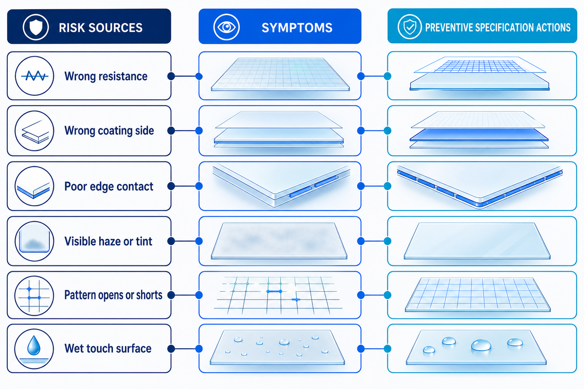
ITO glass projects usually fail when the specification is too generic, the coating side is mishandled, the contact design is weak, or the conductive layer is processed after its limits are already fixed. Most failures are preventable if sheet resistance, patterning, edge contact, cleaning, and inspection are agreed before sampling.[28]
| Failure type | Root cause | Field symptom | Prevention |
|---|---|---|---|
| Wrong resistance | Only “conductive glass” specified | Weak touch response or uneven heating | State target ohms/sq, tolerance, test method, and measurement locations. |
| Wrong coating side | Packaging or drawing unclear | No electrical contact after assembly | Mark side, orientation, and inspection method. |
| Poor edge contact | Busbar area too small | Voltage drop or intermittent signal | Define silver paste, copper tape, clip, or connector plan. |
| Visible haze or tint | Coating target mismatched | Lower display readability | Specify transmittance, haze, and color target. |
| Pattern visibility | Etched and unetched regions reflect differently | Visible electrode grid, moire, or display artifact | Review index matching, low-reflection coating, pitch, and optical bonding. |
| Pattern opens or shorts | Ablation ridge, residue, debris, or incomplete isolation | Dead zone, false touch, adjacent-electrode short, or layer short | Set isolation resistance, residue limits, edge morphology, minimum line/gap, and test coupons. |
| Film damaged by heat process | Strengthening or tempering sequence not matched to coating | Resistance drift or optical loss after processing | Define process order, barrier layer need, and post-process retest. |
| Substrate sodium diffusion | Soda-lime glass annealed without effective diffusion barrier | Higher resistivity, defects, or unstable coating properties | Confirm substrate chemistry, annealing window, and SiO2/Al2O3 barrier design. |
| Wet-bias optical darkening | Electrolyte exposure and negative bias | Transparency loss while resistance still appears acceptable | Add potential window, cycling, optical inspection, and chemistry limits. |
| ESD or touch-module qualification gap | Only material coupon tests specified | Good ITO sheet but unreliable HMI behavior | Define module-level touch, durability, and ESD standards before approval. |
| Wet or contaminated touch surface | Water film, droplets, dust, or cleaning residue on the panel | False touch, missed touch, or unstable multi-touch behavior | Test wet-finger, water-drop, cleaning, dust, and controller rejection criteria by sensing architecture. |
| Display coupling or signal-bandwidth limit | Touch electrodes placed close to display electrodes in a thin stack | Reduced received signal or noisy touch response despite acceptable ITO resistance | Validate touch controller passband, SNR, shielding, grounding, and final display integration. |
| Incomplete optical method | Only one transmittance percent specified | Customer sees haze, reflection, or color shift | State spectral range, regular/diffuse basis, haze, and reflectance target. |
| Scratched conductive layer | Cleaning or handling error | Localized high resistance | Define gloves, separator film, and wash process. |
| Brittle coating response | Film too thick or flexed | Cracking in flexible or stressed use | Avoid bending rigid ITO glass; evaluate alternatives for flex. |
| Bonding conflict | Adhesive and surface energy mismatch | Delamination or bubbles | Test adhesive on the actual coated surface. |
| Supply delay | Indium and coating availability ignored | Prototype cannot scale | Confirm lead time, substitute options, and approved sources. |
How Saiwei Applies ITO Glass in Touch Screen Projects
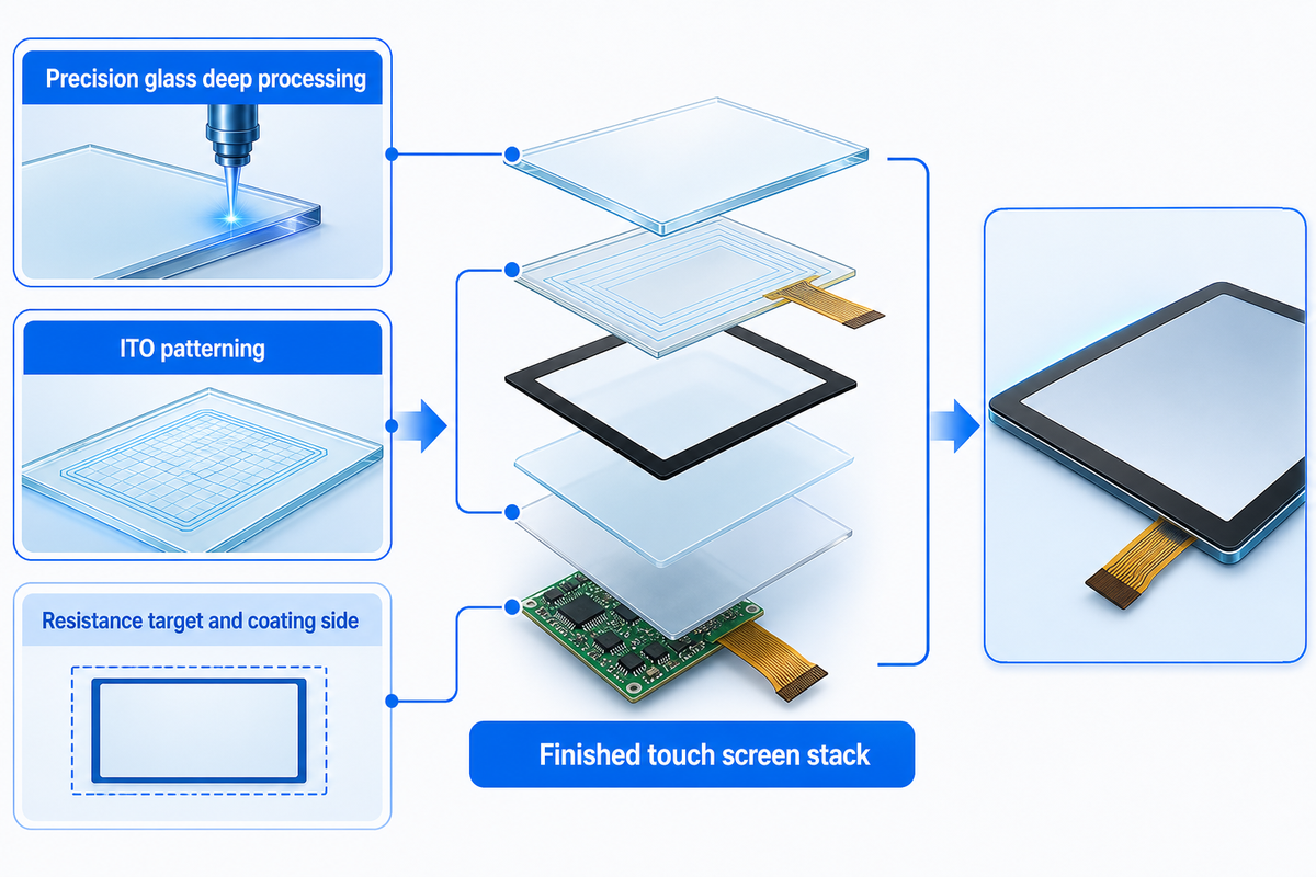
Saiwei Glass is relevant to ITO glass buyers because the company doesn’t treat conductive glass as an isolated sheet. According to its about page, Dongguan Saiwei Glass Co., Ltd. focuses on precision glass deep processing for optical touch screen glass and cover glass, with cutting, CNC, high-precision screen printing, tempering, surface treatment, R&D, production, and after-sales support under one workflow.
That matters because a finished industrial touch screen is a stack, not a raw substrate.[31] Saiwei’s glass manufacturing capabilities and touch glass customization data provide a practical route for engineers who need custom size, 0.55 mm or thicker glass, chemical strengthening, screen printing, laser engraving, ITO patterning, and prototype sampling before mass production.
The ITO layer must work with the cover glass, printed border, optical adhesive, coating package, edge treatment, controller, cable, housing, and inspection plan.
If your drawing already calls for indium tin oxide coated glass, send the resistance target, size, substrate type, coating side, line pattern, operating environment, and downstream assembly plan. If your drawing only says “conductive glass”, define whether the part needs ITO, FTO glass, another transparent conductive oxide, or a plain cover glass with a separate sensor film. That early distinction prevents cost, yield, and touch-response problems later.
Specification Vocabulary Buyers Should Recognize
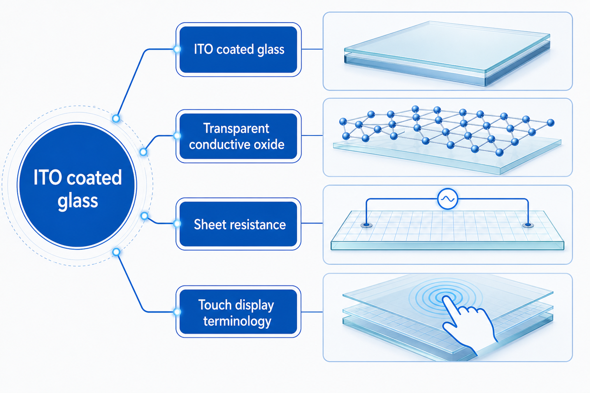
You may see ITO coated, ITO coated glass, indium tin oxide coated glass, ITO glass substrates, ITO substrates, coated glass substrates, coated glass sheet, glass slides, glass sheet, glass plate, quartz, PET substrates, polymer substrates, FTO, FTO glass, AZO, indium zinc oxide, indium-tin-oxide, transparent conductive oxide, transparent conducting oxide, TCO, TCOs, ITO film, standard ITO, high-quality ITO, high-quality ITO glass, transparent conductive glass, transparent conductive layer, transparent electrode, conductive layer, conductor, semiconductor, n-type semiconductor, thin film, thin layer, thin-film photovoltaic, optoelectronic, anti-reflective, optical, optical transparency, transmittance, resistivity, electrical conductivity, electrical resistance, conductivity and transparency, plasma, magnetron, magnetron sputtering, deposition, fabrication, etch, and surface of ITO in drawings, datasheets, and inspection reports.
Related applications of ITO can include OLED displays, organic light-emitting diodes, solar cell electrodes, smart windows, microscopy, scanning electron microscopy sample carriers, conducting polymer films, and research and development devices. The same vocabulary can describe many applications, so the drawing must still define the exact substrate, coating, and inspection values. For touch projects, IEC 62908-1-2:2017 is useful because it treats touch displays, interactive displays, and their components as distinct terminology layers rather than one generic conductive-glass part.[29]
Preguntas frecuentes
Is ITO glass the same as conductive glass?
ITO glass is one type of conductive glass. Conductive glass is a broader category that can include ITO, FTO, AZO, metal mesh, or other conductive layers. If a drawing only says conductive glass, the supplier should confirm the required coating material, sheet resistance, transparency, substrate, and operating environment. For touch-screen buyers, this wording also prevents a cover glass quotation, a sensor glass quotation, and a finished touch-module quotation from being treated as the same part.
How do you check which side of ITO glass is conductive?
The simplest quick check is a multimeter across the surface, but a production acceptance reading should define the method. Four-point-probe measurement reduces contact-resistance error and can be mapped across the coated area. Record probe spacing, sample location, acceptance limit, and coating-side label in the inspection sheet. The coated side should show measurable conductivity; the plain glass side shouldn’t. For production, mark orientation in the drawing and packaging instructions so the coating side isn’t reversed during printing, bonding, or assembly.
What is a good sheet resistance for ITO touch screen glass?
There is no universal best value. Touch screen glass often falls somewhere inside ranges such as 10-300 ohms/sq, but the correct target depends on panel size, sensor layout, controller, optical target, and stack design. Lower resistance can help signal response, but it may not be the best optical or cost choice.
For example, a small control panel may care more about clean pattern isolation and low haze, while a large projected-capacitive panel may need tighter uniformity mapping and stronger edge-contact design. Ask the supplier to quote the resistance tolerance, measurement method, coating side, busbar plan, and any module-level touch tests together; otherwise two parts with the same nominal ohms/sq can behave differently after bonding.
Can ITO glass be laser cut or etched?
ITO patterns can be created by etching or laser processes, but the method must match the film, substrate, line width, and downstream assembly. A supplier should review minimum gaps, edge contact, inspection coupons, and cosmetic requirements before committing to mass production.
Can ITO glass be tempered after coating?
Do not assume it can. High-temperature strengthening after ITO deposition can change electrical and optical properties unless the process, barrier layer, and coating design are built for it. If the part needs strengthened glass, ask the supplier to confirm the sequence and provide post-process sheet-resistance and optical results.
Why is indium supply discussed in ITO projects?
Indium risk should be described precisely. USGS treats indium as a critical mineral and notes that it’s typically recovered from sphalerite, a zinc-sulfide mineral; a 2022 USGS update also says quantitative data about U.S. indium occurrence and recovery is limited and that the United States was 100 percent net import reliant in 2021.[22] For custom industrial projects, that supply context makes lead time, approved alternatives, and price validity worth checking early.
When should buyers choose FTO or AZO instead of ITO?
FTO may be considered when high-temperature durability or certain chemical conditions matter. AZO may be explored when indium cost or availability is a concern. ITO remains common for transparent conductive glass, but the best choice depends on transparency, conductivity, process temperature, humidity, flexibility, and module economics.
Referencias y fuentes
- A Review of Transparent Conducting Films (TCFs): Prospective ITO and AZO Deposition Methods and Applications
- A Brief Review of Transparent Conducting Oxides (TCO): The Influence of Different Deposition Techniques on the Efficiency of Solar Cells
- Touch-responsive indium tin oxide is very thin and flexible
- High temperature reactive ion etching of indium-tin oxide
- US8049862B2: Indium tin oxide (ITO) layer forming
- USGS: Indium
- IEEE Spectrum: The Trouble With Touch Screens
- ASTM Glass Standards and Ceramic Standards
- Rapid thermal annealing of ITO films
- BYU Cleanroom: Four Point Probe and Two Point Probe Measurements
- NIST: Four Dimensions 280DI Sheet Resistance Mapping System
- Optics Express: Moire-free fingerprint sensors based on multilayer oxide-metal-oxide electrodes
- Use of and Occupational Exposure to Indium in the United States
- ISO 15368:2021: Measurement of reflectance and transmittance of plane optical components
- Effects of surface compression strengthening on properties of indium tin oxide films deposited on automobile glass
- Advancements in Transparent Conductive Oxides for Photoelectrochemical Applications
- Highly Transparent Conducting Indium Tin Oxide Thin Films Prepared by Radio Frequency Magnetron Sputtering and Thermal Annealing
- Ridge Minimization of Ablated Morphologies on ITO Thin Films Using Squared Quasi-Flat Top Beam
- Characterization of Indium Tin Oxide (ITO) Thin Films towards Terahertz (THz) Functional Device Applications
- NIST: Heaters based on ITO Thin films
- On-screen fingerprint sensor with optically and electrically tailored transparent electrode patterns for use on high-resolution mobile displays
- USGS Updates Mineral Database with Indium Deposits in the United States
- Effect of barrier layers on the properties of indium tin oxide thin films on soda lime glass substrates
- Monitoring the Electrochemical Failure of Indium Tin Oxide Electrodes via Operando Ellipsometry Complemented by Electron Microscopy and Spectroscopy
- Silver Meshes for Record-Performance Transparent Electromagnetic Interference Shielding
- IEC 62908-12-10:2025
- IEC 62908-13-10:2016
- IEC 61000-4-2:2025
- IEC 62908-1-2:2017
- IEC 62908-12-20:2019
- Development and Experimental Comparison of Low-Cost, Reliable Capacitive Touch Sensing Boards
- Revisión de tecnologías de pantalla táctil capacitivas: descripción general, tendencias de investigación y enfoques de aprendizaje automático
- Mutual Capacitive Sensing Touch Screen Controller for Ultrathin Display with Extended Signal Passband Using Negative Capacitance